Wafer back surface treating method and dicing sheet adhering apparatus

a back surface treatment and adhesion technology, applied in the direction of electrical equipment, semiconductor/solid-state device manufacturing, basic electric elements, etc., can solve the problems of severe contamination of dicing sheet and disabled pick-up

Inactive Publication Date: 2007-05-15
NITTO DENKO CORP
View PDF4 Cites 5 Cited by
  • Summary
  • Abstract
  • Description
  • Claims
  • Application Information

AI Technical Summary

Benefits of technology

[0042]In order to evaluate an effect of a deactivation treatment, wafers each were ground to a thickness of 400 μm with Back Grinder DFG-840 manufactured by DISCO Inc., a deactivation treatment was applied to the wafers and UV-setting adhesive sheets prepared separately were adhered to the wafers within 1 hr of the deactivation treatment. One of the wafers was illuminated with UV 30 min after adherence of the sheet with UV illuminating apparatus UM-810 manufactured by Nitto Denko Corporation and a UV-setting adhesive sheet was adhered on only one of the wafers subjected to a treatment with UV illumination mechanism exhaust 3 hr after the deactivation treatment. Measurement of a sticking force was conducted on the wafers treated as described above. In the deactivation treatment, gases other than the UV illumination mechanism exhaust were all blown to wafers at a flow rate of 1 L / min. Only of the UV illumination mechanism exhaust was blown to a wafer at a flow rate of 3 L / min. One wafer was diced with Dicer DFD-651 manufactured by DISCO Co. into pieces each of 5 mm×7 mm and UV illumination was applied to the pieces with UV illuminating apparatus UM-810 manufactured by Nitto Denko Corporation, followed by a picking-up evaluation.
[0043](1) Measurement of Sticking Force
[0044]A releasing force of an adhesive tape was measured at a pulling angle of 15 degrees with a pulling tester in which the pulling angle is arbitrarily adjustable and can keep at a constant value.
[0046]Picking-up was conducted in conditions of 4 pins and a plunge-up of 500 μm with Dibonder CPS-100 manufactured by NEC Machinery Co., Ltd.
[0047]A UV-setting adhesive sheet for evaluation was prepared as follows:

Problems solved by technology

In a case where, in this way, a dicing sheet is adhered to a wafer a few hours after the end of polishing, or a process from a wafer polishing apparatus to a dicing sheet adhering apparatus is integrated into a single system, so a dicing sheet is adhered to the wafer immediately after the end of polishing, a sticking force between the dicing sheet and the back surface of a wafer increases, which has led to a possibility to cause a problem that when semiconductor chips obtained by being separated into small pieces are picked up after the dicing step, the picking-up is disabled or contamination by the dicing sheet is severe even if the picking-up is enabled.

Method used


Image

  • Wafer back surface treating method and dicing sheet adhering apparatus
  • Wafer back surface treating method and dicing sheet adhering apparatus
  • Wafer back surface treating method and dicing sheet adhering apparatus

Examples


example 1

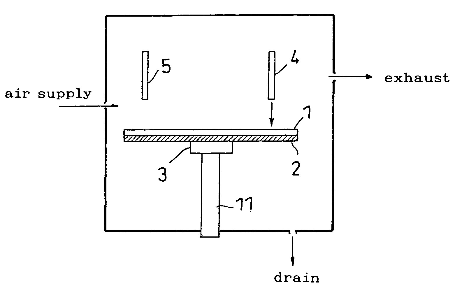
[0050]FIG. 1 is an example of a wafer back surface cleaning section of a grinding or polishing apparatus related to the invention. In FIG. 1, a wafer 1, in a state where a back grinding tape 2 remains stuck thereon, is fixed on a rotary shaft 11 by vacuum suction with a suction pad 3 interposed therebetween and cleaned with a cleaning water spraying nozzle 5 while being rotated about the rotary shaft 11, and thereafter, removal of water and a deactivation treatment by ozone are simultaneously performed with an ozone blowing nozzle 4. Ozone is produced by an ozone generator provided separately. An ozone concentration is preferably in the range of from 0.1 through 10 ppm in consideration of a time necessary for reduction in ozone concentration when the apparatus is opened. Exhaust is effected by a common exhaust means such as a blower or the like. The wafer is unloaded through a wafer take-out port by a robot arm having a wafer sucking means after an ozone concentration is reduced to ...

example 2

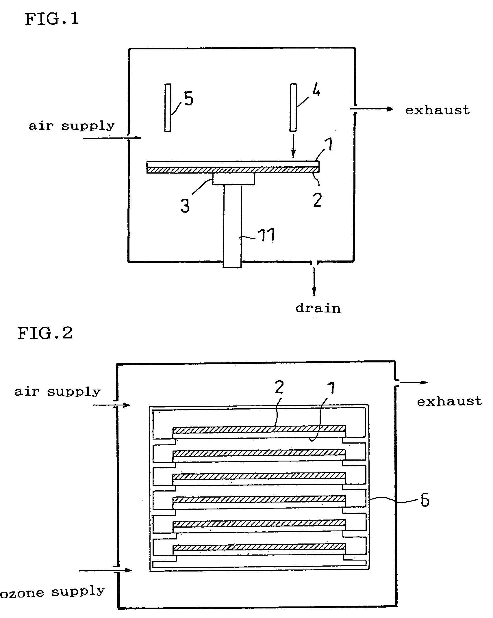
[0051]FIG. 2 is an example of a treatment by ozone of a wafer cassette related to the invention. In FIG. 2, wafers 1 are housed in a wafer cassette 6, each being in a state where the back grinding tape 2 remains stuck thereon. The wafer cassette 6 is placed in a vessel having an ozone supply section and an exhaust section. Wafers 1 are subjected to a deactivation treatment in the condition similar in Example 1. The cassette is taken out from the closed vessel, opening the top portion thereof after an ozone concentration is reduced through 0.1 ppm or less while air is supplied through an air supply port.

example 3

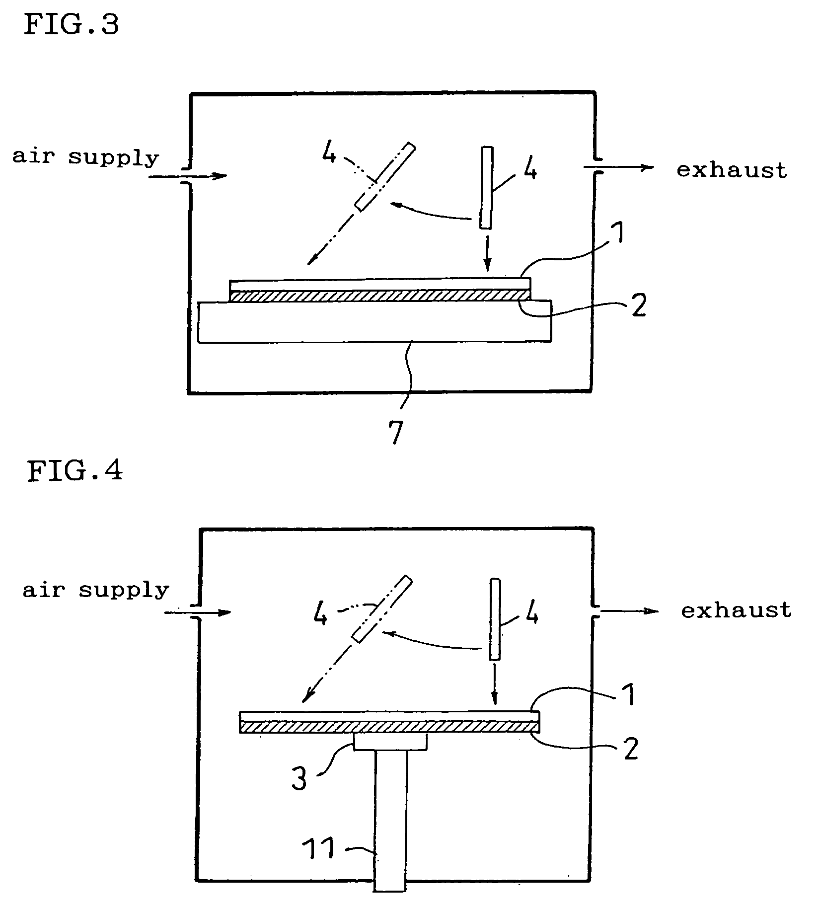
[0052]FIG. 3 is an example of a treatment by ozone of wafers, sheet-fed, related to the invention. In FIG. 3, a wafer 1, in a state where a back grinding tape 2 is not stuck thereon, is fixed to a chuck table 7. An ozone blowing nozzle 4 is mounted to a movable shaft so that a blowing direction is able to be directed to any position on the wafer 1 and ozone can be blown to across all of the surface by proper movement thereof. A treatment condition and take-out method are similar to those in Example 1.


PUM


Abstract

Provided is a treatment method of a semiconductor wafer facilitating picking-up of semiconductor chips and preventing contamination by a dicing sheet. A wafer back surface treating method is characterized in that a ground or polished surface of a semiconductor wafer activated in a grinding or polishing step, with semiconductor circuits formed thereon, is deactivated. In the method, the activation treatment with an oxidizing agent is preferable. Furthermore, the activation treatment is preferably implemented with blowing of ozone to a ground or polished surface of a wafer, with ozone water or with illumination of a ground or polished surface of a wafer with ultraviolet (UV). It is preferable to adhere a dicing sheet after the deactivation treatment.

Description

BACKGROUND OF THE INVENTION[0001]1. Field of the Invention[0002]The invention relates to a treatment method of a semiconductor wafer (hereinafter referred to as wafer), which is especially useful as a treatment method applied to a process including a step of adhering a dicing sheet to the wafer, following a grinding step for thinning the wafer (or one of various kinds of polishing steps) after circuits are formed on the wafer; and to an apparatus using the treatment method of the wafer.[0003]2. Prior Art[0004]A semiconductor wafer made of silicon, gallium, arsenide or the like has been conventionally used in a way such that circuits are formed on the wafer, thereafter a grinding step for thinning the wafer is applied thereto, then a dicing sheet is adhered thereto and the wafer with the sheet is then diced into small device pieces, followed by a mounting step (see, for example, JP-A No. 2003-7646). In such a process, since steps including as far as polishing or back grinding of a ba...

Claims


Application Information

Patent Timeline
Patent Type & Authority Patents(United States)
IPC IPC(8): H01L21/30H01L21/46H01L21/304H01L21/301H01L21/306H01L21/68H01L21/78
CPCH01L21/02057H01L21/6835H01L21/78
Inventor OKAWA, YUJI
Owner NITTO DENKO CORP
Why Eureka
Try Eureka