Power semiconductor device

a technology of semiconductor devices and semiconductors, applied in the direction of electric variable regulation, process and machine control, instruments, etc., can solve the problems of reducing the accuracy of measurement, increasing the load on the cpu, and affecting the real time property, so as to achieve the effect of increasing the accuracy of measuremen

Active Publication Date: 2007-05-15
MITSUBISHI ELECTRIC CORP
View PDF10 Cites 2 Cited by
  • Summary
  • Abstract
  • Description
  • Claims
  • Application Information

AI Technical Summary

Benefits of technology

[0012]It is an object of the present invention to provide a power semiconductor device capable of increasing the accuracy of measurement.
[0014]The power semiconductor device according to the present invention eliminates the need to use an interrupt function of the CPU. This avoids the increase in load on the CPU, thereby producing the effects of preventing a real time property from being impaired and preventing the accuracy of measurement from decreasing. Additionally, the power semiconductor device according to the present invention eliminates the need to use an input capture function of the CPU to produce the effect of placing no strain on channels for the input capture.

Problems solved by technology

However, the use of the interrupt function is disadvantageous in that the increased load on the CPU impairs a real time property or decreases the accuracy of measurement.
The use of the input capture function, which is normally used to read an encoder, is disadvantageous in that there are not enough channels to read pulses from the HVIC.
This presents a problem such that the accuracy of measurement might decrease.
If the reference frequency of the reference clock is 10 MHz and a full scale current value is 500 A, increased error of 500 A×(40 kHz / 10 MHz)=2A results in the low accuracy of measurement.
This presents a problem that the response is slow in some cases.
It is, therefore, more difficult for the power semiconductor device employing the shunt resistor and the HVIC for current detection to make corrections and, accordingly, to increase gain than the power semiconductor device employing the Hall element which exhibits the smaller variations for current detection.

Method used


Image

  • Power semiconductor device
  • Power semiconductor device
  • Power semiconductor device

Examples


Embodiment Construction

[0020][First Preferred Embodiment]

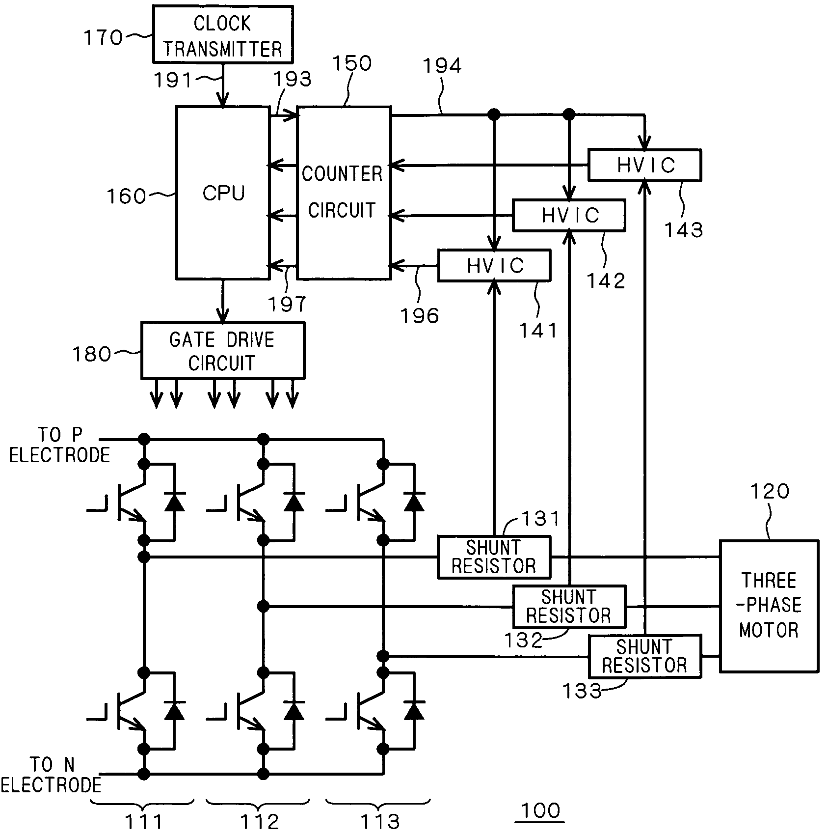
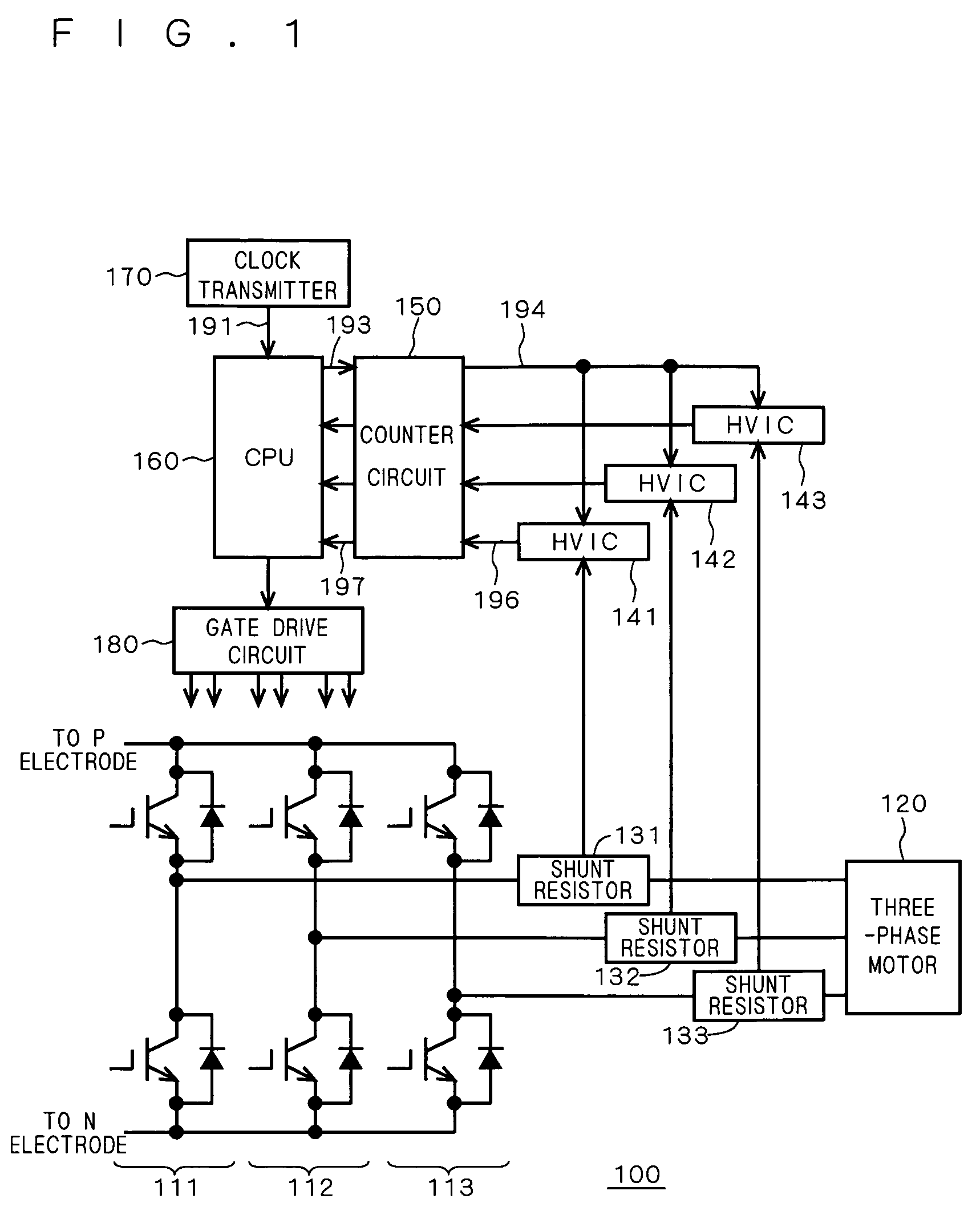
[0021]FIG. 1 shows the construction of a power semiconductor device 100 according to a first preferred embodiment of the present invention.

[0022]Referring to FIG. 1, inverter circuits 111 to 113 are connected to a P electrode and an N electrode, and supply current to the U, V and W phases, respectively, of a three-phase motor 120 to control the same. The inverter circuits 111 to 113 are connected to the three-phase motor 120 through shunt resistors 131 to 133, respectively. The shunt resistors 131 to 133 are connected to HVICs 141 to 143, respectively. The HVICs 141 to 143 are connected to a counter circuit 150. The counter circuit 150 is connected to a CPU 160. The CPU 160 is connected to a clock transmitter 170 and a gate drive circuit 180.

[0023]With reference to FIG. 1, voltages are developed across the respective shunt resistors 131 to 133, based on currents flowing to the U, V and W phases of the three-phase motor 120.

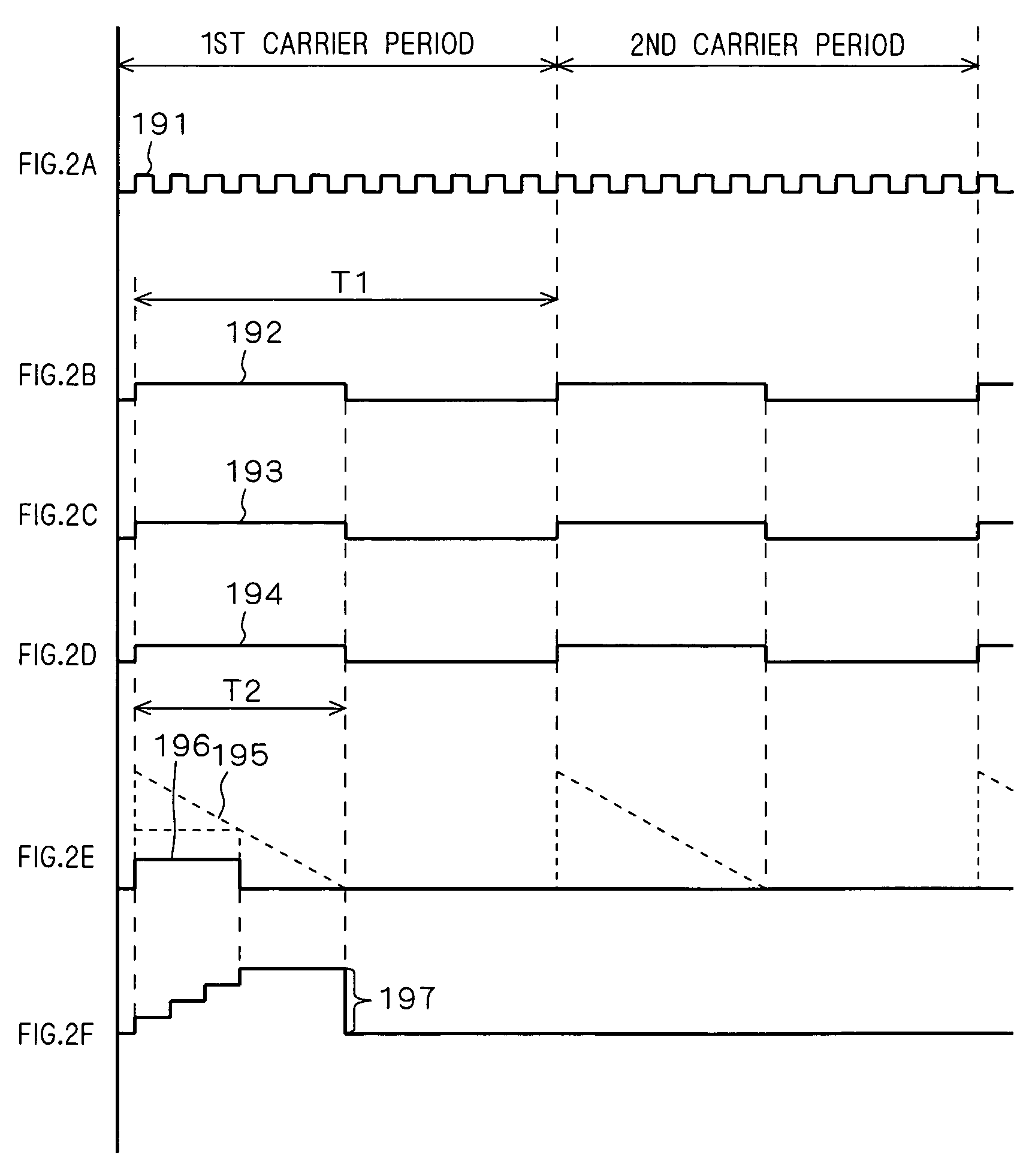
[0024]The operation of the...


PUM


Abstract

Inverter circuits are connected to a P electrode and an N electrode, and control the U, V and W phases, respectively, of a three-phase motor. The inverter circuits are connected to the three-phase motor through shunt resistors, respectively. The shunt resistors are connected to HVICs, respectively. The HVICs are connected to a counter circuit. The counter circuit is connected to a CPU. The CPU is connected to a clock transmitter and a gate drive circuit.

Description

BACKGROUND OF THE INVENTION[0001]1. Field of the Invention[0002]The present invention relates to a power semiconductor device and, more particularly, to a technique for detecting the load current of a motor for an automotive vehicle, and the like.[0003]2. Description of the Background Art[0004]Background art current detection of power semiconductor devices for driving motors for automotive vehicles and the like has generally employed a Hall element or a combination of a shunt resistor and a linear isolation amplifier. Recently, a power semiconductor device employing a combination of a shunt resistor and an HVIC (high voltage IC) has made its appearance as a less expensive power semiconductor device than those described above. The HVIC is a control element which performs inverse level shift from a voltage on the high side of the shunt resistor to a voltage on the low side thereof, and has a PWM (pulse width modulation) function for converting the value of a voltage developed across t...

Claims


Application Information

Patent Timeline
Patent Type & Authority Patents(United States)
IPC IPC(8): H02M7/5387H02M3/24H02P5/34H02H7/10H02M7/48H02P27/06
CPCH02M7/53873
Inventor SHINOHARA, MASUO
Owner MITSUBISHI ELECTRIC CORP
Why Eureka
Try Eureka