Planar waveguide with patterned cladding and method for producing the same

a technology of patterned cladding and planar waveguide, which is applied in the direction of optical waveguide light guide, instruments, optics, etc., can solve the problems of reflection loss, difficult handling, limited applicability, etc., and achieve the effect of avoiding mechanical damage and scattering loss

Inactive Publication Date: 2007-05-15
ZETTA RES & DEV LLC RPO SERIES
View PDF25 Cites 82 Cited by
  • Summary
  • Abstract
  • Description
  • Claims
  • Application Information

AI Technical Summary

Benefits of technology

[0029]Also, while the present invention discloses that certain side or end regions of the light transmissive portion be left unclad, those skilled in the art will understand that apart from the functional regions of interest, the light transmissive core is best clad as much as possible to avoid mechanical damage and scattering losses.

Problems solved by technology

One solution is to use a discrete element such as a ball lens or a cylindrical gradient refractive index (GRIN) lens, however such lenses are difficult to handle because of their small size, require precise alignment in two dimensions, and introduce additional interfaces (with inherent reflection losses).
They are, however, limited in their applicability, relying on differential etch rates between the cladding (e.g. silica) and the core (e.g. germanium-doped silica).
For example, selective chemical etching generally cannot be used for polymer-based integrated optical waveguides.
Furthermore, the thermal rounding process can only be used if the core material has a softening point, which excludes non-thermoplastic polymers and crystalline materials such as silicon and other semiconductors.
A further disadvantage with chemical etching-based techniques is that the lens structures can only be prepared after the optical waveguide circuit chips have been diced (cutting or breaking into individual chips).
While many chips can be collected and etched at the same time, this still requires careful handling and extra process steps.
Without wishing to be bound by theory, it is well known that introducing a bend into an optical waveguide perturbs the guided modes such that they tend to leak out the side of the bend, resulting in loss of optical power.
For large bend radii (i.e. gradual bends) this loss is negligible, but as the bend radius is reduced, there comes a point where the loss becomes unacceptable.
A disadvantage with omitting the upper cladding in planar waveguides is that the mechanical strength of the structure may be insufficient, i.e. the structure cannot be processed and handled using standard techniques.
Also, bare core structures are extremely vulnerable to mechanical damage or to the formation of scattering centres by extraneous dust.

Method used


Image

  • Planar waveguide with patterned cladding and method for producing the same
  • Planar waveguide with patterned cladding and method for producing the same
  • Planar waveguide with patterned cladding and method for producing the same

Examples


example 1

[0108]Following the procedure disclosed in U.S. patent application Ser. No. 10 / 308562, a lower refractive index polymer A was prepared with a viscosity of 2500 cP (at 20° C.) and a refractive index (measured at 20° C. on an Abbe refractometer with room light) of 1.483. A higher refractive index polymer B was prepared with a viscosity of 2200 cP (at 20° C.) and a refractive index of 1.509 (at 20° C.). A suitable photoinitiator was added to both polymer A and polymer B.

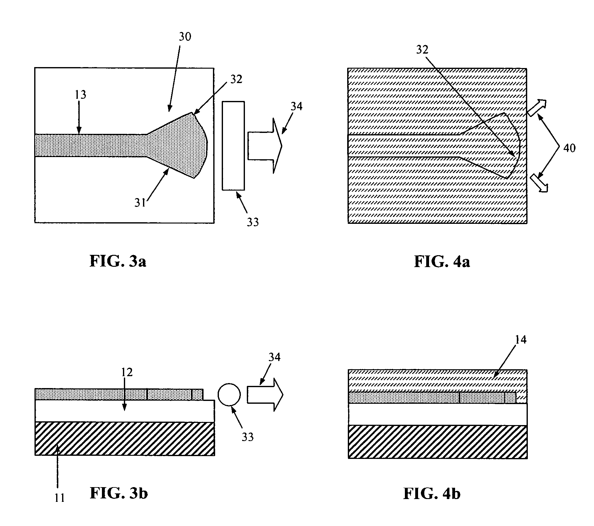
[0109]Polymer A was spin coated onto a silicon wafer and cured with UV light from a mercury lamp, to form a lower cladding layer 20 μm thick and with a refractive index of 1.478 (at 20° C. and 1550 nm). Polymer B was spin coated onto the lower cladding, and patterned with UV light through a mask; the unexposed polymer B material was then dissolved in isopropanol to form a core and unitary lens structure as shown in FIG. 3a. The core was 8 μm wide and 15 μm high, and had a refractive index of 1.505 (at 20° C. and 1550 nm...

example 2

[0111]Polymer A from Example 1 was spin coated onto a silicon wafer and cured with UV light from a mercury lamp, to form a lower cladding layer 20 μm thick and with a refractive index of 1.478 (at 20° C. and 1550 nm). Polymer B from Example 1 was spin coated onto the lower cladding, and patterned with UV light through a mask; the unexposed polymer B material was then dissolved in isopropanol to form a core with four tight bends as shown in FIG. 8. The core was 8 μm wide and 15 μm high, and had a refractive index of 1.505 (at 20° C. and 1550 nm). Finally, polymer A was spin coated over the core and patterned with UV light through a mask; the unexposed polymer A material was then dissolved in isopropanol to form a patterned upper cladding as shown in FIG. 10.

example 3

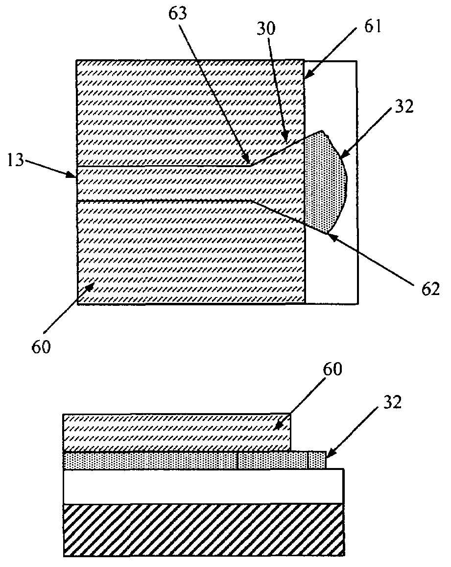
[0112]Polymer A was meniscus coated onto an acrylic substrate (Perspex, or polymethylmethacrylate), and cured with UV light from a mercury lamp, to form a lower cladding layer 10 μm thick and with a refractive index of 1.478 (at 20° C. and 1550 nm). Polymer B was meniscus coated onto the lower cladding, and patterned with UV light using a scanning projection aligner; the unexposed polymer B material was then dissolved in isopropanol to form a core and unitary lens structure as shown in FIG. 3a. The core was 8 μm wide and 20 μm high, and had a refractive index of 1.505 (at 20° C. and 1550 nm). Finally, polymer A was meniscus coated over the core and patterned with a scanning projection aligner; the unexposed polymer A material was then dissolved in isopropanol to form a patterned upper cladding as shown in FIG. 6a.


PUM


Abstract

Integrated optical waveguides and methods for the production thereof which have a patterned upper cladding with a defined opening to allow at least one side or at least one end of a light transmissive element to be air clad. The at least one side or at least one end is, for preference, a lens structure unitary with the waveguide, or a bend.

Description

FIELD OF THE INVENTION[0001]The invention relates to an integrated optical waveguide with a patterned upper cladding, and to methods for patterning the upper cladding.BACKGROUND OF THE INVENTION[0002]Integrated optical waveguides typically consist of a patterned, light guiding core layer (of refractive index n1) surrounded by a cladding material (of refractive index n2, where n2<n1) and mounted on a mechanically robust substrate. These waveguides generally have flat end faces, often produced by cutting the substrate and waveguide structure with a dicing saw, followed by a polishing step to remove scattering centres. Light propagating along the waveguide is guided within the core by the refractive index difference between core and cladding.[0003]Referring to the drawings, FIGS. 1a and 1b show side and end views of the end face of a typical integrated optical waveguide 10 as known in the art, comprising a substrate 11, a lower cladding layer 12, a light guiding core 13 and an upper...

Claims


Application Information

Patent Timeline
Patent Type & Authority Patents(United States)
IPC IPC(8): G02B6/32G02B6/10G02B6/122G02B6/124G02B6/138
CPCG02B6/1228G02B6/138G02B6/1245G02B6/12
Inventor MAXWELL, IAN ANDREWKUKULJ, DAXCHARTERS, ROBERT B.
Owner ZETTA RES & DEV LLC RPO SERIES
Why Eureka
Try Eureka