Testing CMOS CAM with redundancy

a technology of cmos cam and redundancy, applied in the field of cmos cam ternary content addressable memory (tcam) devices, can solve the problems of time-consuming and costly testing, data corruption by memory device use,

Inactive Publication Date: 2007-05-15
MICRON TECH INC
View PDF6 Cites 11 Cited by
  • Summary
  • Abstract
  • Description
  • Claims
  • Application Information

AI Technical Summary

Problems solved by technology

Although testing is time consuming and costly, testing is required to identify errors in the device.
If errors are not identified, the use of the memory device can corrupt data.

Method used


Image

  • Testing CMOS CAM with redundancy
  • Testing CMOS CAM with redundancy
  • Testing CMOS CAM with redundancy

Examples


Embodiment Construction

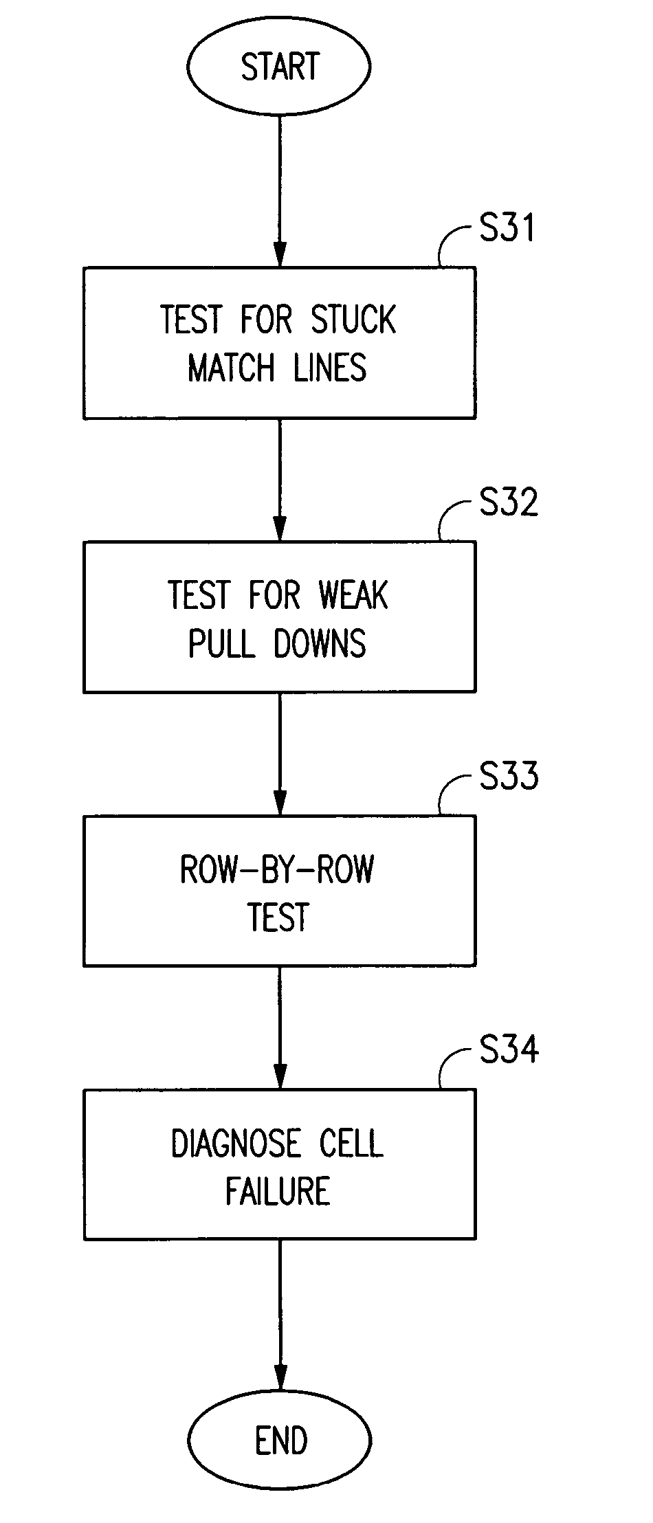
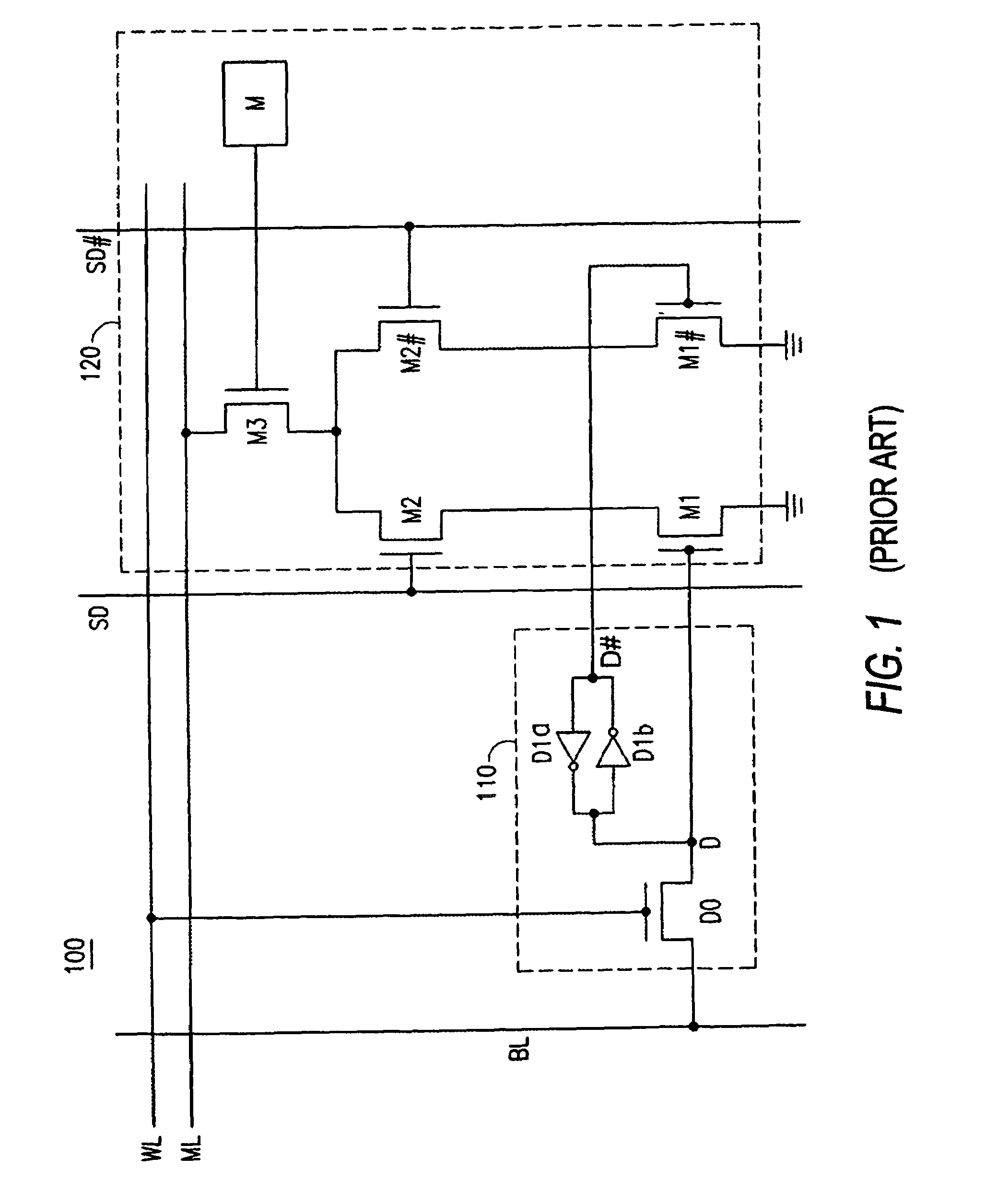
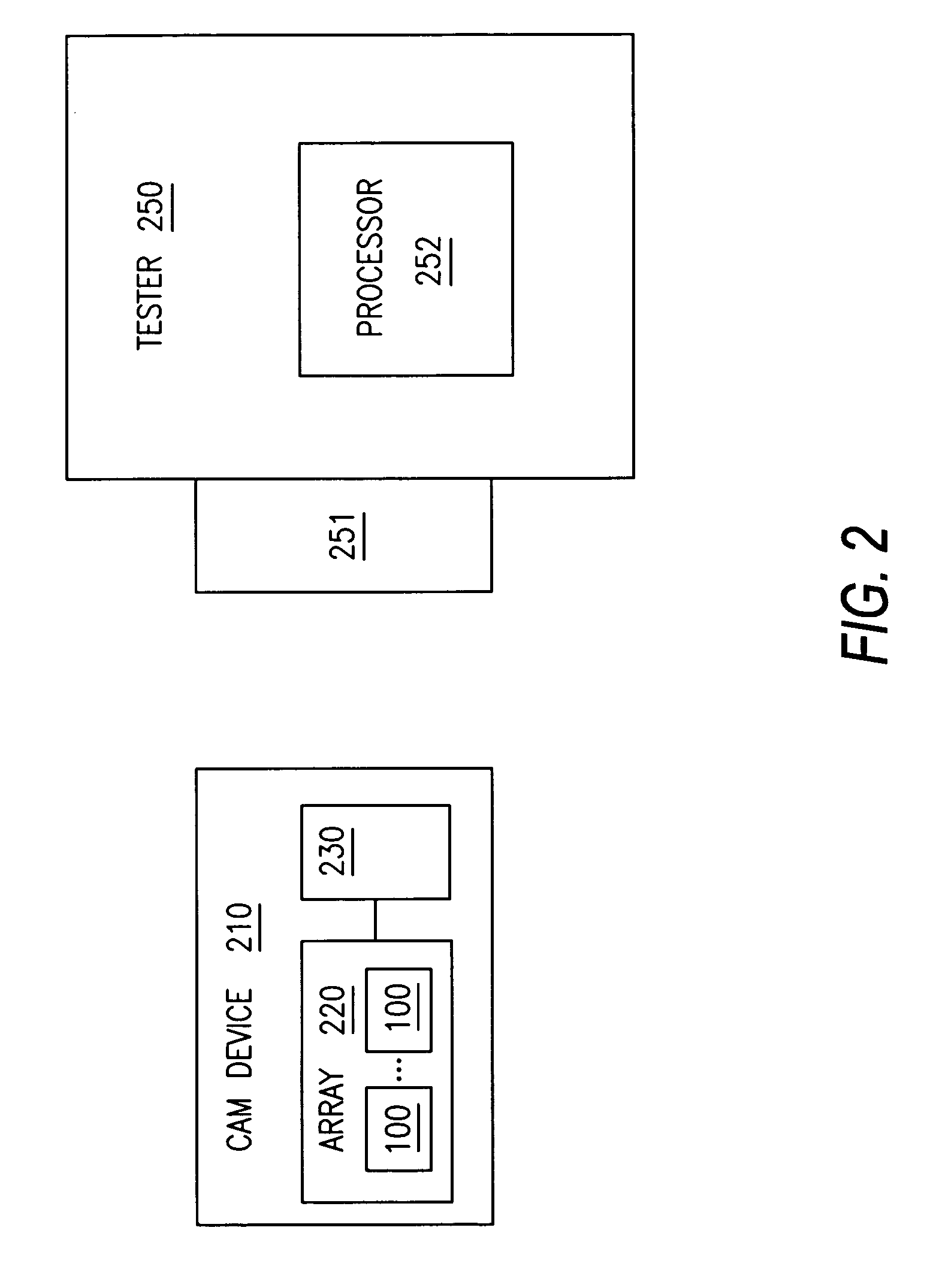
[0021]Now referring to the drawings, where like reference numerals designate like elements, there is shown in FIG. 2 a CAM device 210 and a tester 250. The CAM device 210 includes at least one memory array 220. Each array 220 has a plurality of CAM cells 100 (FIG. 1). The CAM device 210 also includes a control circuit 230 for operating the CAM device 210 and for interfacing with external devices. The tester 250 includes an interface 251 for communicating with the CAM device 210. The tester 250 further includes a processor 252, which can execute a series of tests on the CAM device 210 as described below with reference to FIGS. 3–5, 6A, and 6B. The tester 250 tests the device 210 by placing the device 210 into a test mode and then executing the below described procedure. The device 210 may be placed into test mode in a variety of ways which are well known, such as asserting a signal on a test mode enable pin (such pins are typically made non accessible after the device 210 has been te...


PUM


Abstract

A method for testing an CMOS ternary content addressable memory (TCAM) device includes a match line test to identify stuck match lines, a pull down test to identify weak pull downs (from the match line to ground), and a row-by-row match test. During the row-by-row match test a failed cell can be repaired or the row associated with the failed cell can be disabled. A failed cell or its associated row can also be repaired or disabled, respectively, after the test. Additionally, individual CAM cells which are identified as being defective can be further tested to identify which component of the CAM cell failed.

Description

FIELD OF INVENTION[0001]The present invention relates generally to semiconductor memory devices and, more particularly to a method for testing CMOS Ternary Content Addressable Memory (TCAM) devices. The present invention may also be used to test binary content addressable memory (CAM) devices.BACKGROUND OF THE INVENTION[0002]An essential semiconductor device is semiconductor memory, such as a random access memory (RAM) device. A RAM allows a memory circuit to execute both read and write operations on its memory cells. Typical examples of RAM devices include dynamic random access memory (DRAM) and static random access memory (SRAM).[0003]Another form of memory is the content addressable memory (CAM) device. A CAM is a memory device that accelerates any application requiring fast searches of a database, list, or pattern, such as in database machines, image or voice recognition, or computer and communication networks. CAMs provide benefits over other memory search algorithms by simulta...

Claims


Application Information

Patent Timeline
Patent Type & Authority Patents(United States)
IPC IPC(8): G11C29/00G11C15/00G11C29/02G11C29/12
CPCG11C15/00G11C29/02G11C29/12
Inventor MANTRI, PRASAD
Owner MICRON TECH INC
Why Eureka
Try Eureka