Ion source and ion implanter having the same

a technology of ion source and ion implanter, which is applied in the direction of ion beam tubes, instruments, nuclear engineering, etc., can solve the problems of reducing the emission rate of ion source and filament deterioration, and achieve the effect of suppressing the deterioration of the electron-emitting portion and reducing the electrical resistance of the connection portion

Inactive Publication Date: 2007-05-22
SAMSUNG ELECTRONICS CO LTD
View PDF9 Cites 4 Cited by
  • Summary
  • Abstract
  • Description
  • Claims
  • Application Information

AI Technical Summary

Benefits of technology

[0011]The present invention provides an ion source including a filament that has long endurance by suppressing deterioration of the filament by thermal stress.
[0016]A first coil for suppressing deterioration of the electron-emitting portion due to thermal stresses is wound around the electron-emitting portion. A pair of second coils for reducing electrical resistances of the connection portions is wound around the connection portions. The second coil has a diameter greater than the first coil. Preferably, the filament rod and the first second coils may include tungsten or tantalum.
[0017]The electrons are mainly emitted from the electron-emitting portion rather than the connection portions due to the resistance difference between the electron-emitting portion and the connection portions. As a result, the filament may have long endurance so that downtime of the ion implanter may be decreased.
[0023]According to still another embodiment of the present invention, a filament includes an electron-emitting portion, a pair of leads, a pair of connection portions, a first coil and a pair of second coils. The electron-emitting portion for emitting electrons into an arc chamber is disposed in the arc chamber. The connection portions extend into the arc chamber through the sidewall. The connection portions are connected between the electron-emitting portion and the leads. The first coil is wound around the electron-emitting portion. The first coil suppresses deterioration of the electron-emitting portion by thermal stress. The second coils are wound around the connection portions. The second coils reduce electrical resistances of the connection portions relatively compared to that of the electron-emitting portion. The second coils also have a diameter greater than the first coil.

Problems solved by technology

During emitting the electrons, the filament may be deteriorated due to thermal stress caused by high temperature.
The deterioration of the filament decreases the emission rate of the ion source.

Method used


Image

  • Ion source and ion implanter having the same
  • Ion source and ion implanter having the same
  • Ion source and ion implanter having the same

Examples


Embodiment Construction

[0036]The present invention now will be described more fully hereinafter with reference to the accompanying drawings in which embodiments of the invention are shown.

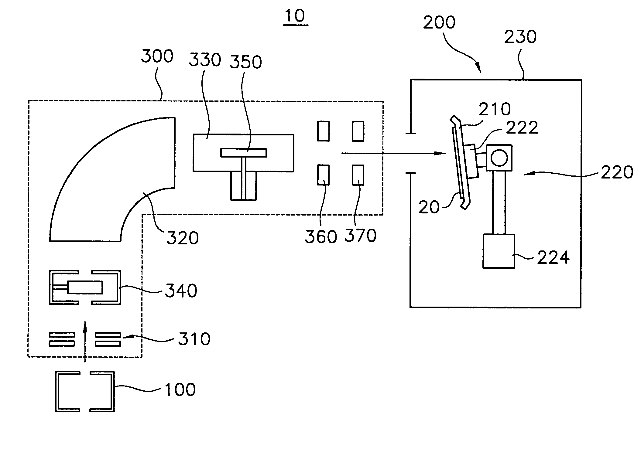
[0037]Referring to FIG. 1, an ion implanter 10 includes an ion source 100 for generating ions that are subsequently implanted into a surface portion of a semiconductor substrate 20, an end station unit 200 for handling a semiconductor substrate 20 for implanting the ions generated from the ion source 100 into the surface portion of the semiconductor substrate 20, and a transportation unit 300, connected between the ion source 100 and the end station unit 200, for transferring the ions to the end station unit 200.

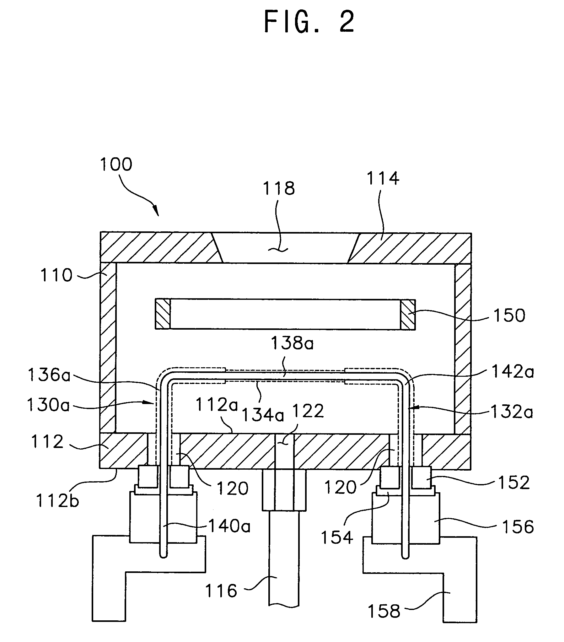
[0038]The ion source 100 includes an arc chamber (not shown) for providing a space in which the ions are generated and at least one filament (not shown) for emitting electrons into the arc chamber. A source gas, including a material that is implanted into the surface portion of the semiconductor substrate 20, is ...


PUM


Abstract

A filament includes a filament rod having an electron-emitting portion, a pair of leads, and a pair of connection portions. The electron-emitting portion is disposed in the arc chamber. The leads extend from the sidewall of the arc chamber to the outside of the arc chamber. The leads are connected to a filament power source. The connecting portions extend from the sidewall of the arc chamber to the inside of the arc chamber. The connection portions are connected between the electron-emitting portion and the leads. The connection portions have an electrical resistance less than that of the electron-emitting portion. Thus, electrons are thermoelectrically emitted into the arc chamber from the electron emission portion rather than the connection portions. An electron emission rate may also be increased. In addition, since the filament has a longer useful life, downtime of an ion implanter including the ion source may be decreased.

Description

CROSS REFERENCE TO RELATED APPLICATION[0001]This application claims priority under 35 USC § 119 to Korean Patent Application No. 2003-0093546, filed on Dec. 19, 2003, the content of which is herein incorporated by reference in its entirety for all purposes.BACKGROUND OF THE INVENTION[0002]1. Field of the Invention[0003]The present invention relates to an ion source and to an ion implanter that includes the ion source. More particularly, the present invention relates to an ion source for generating ions (dopants) that are doped into a surface portion of a semiconductor substrate in processes for fabricating a semiconductor device, and an ion implanter that includes the aforementioned ion source.[0004]2. Description of the Related Art[0005]In general, a semiconductor device is manufactured by a fabrication process for forming an electrical circuit on a silicon wafer that is used for a semiconductor substrate, an electrical die sorting (EDS) process for testing electrical characteristi...

Claims


Application Information

Patent Timeline
Patent Type & Authority Patents(United States)
IPC IPC(8): H01J37/08H01J37/317H01J27/08H01L21/265
CPCH01J37/08H01J37/3171H01J2237/082H01L21/265
Inventor JOO, YOUNG-BYEONG
Owner SAMSUNG ELECTRONICS CO LTD
Why Eureka
Try Eureka