Liquid crystal display device and driving control method thereof

a technology of liquid crystal display panel and control method, which is applied in the direction of instruments, computing, electric digital data processing, etc., can solve the problems of reduced display quality, reduced display quality, and low reliability of liquid crystal display device, and achieve excellent display quality

Inactive Publication Date: 2007-05-22
CASIO COMPUTER CO LTD
View PDF24 Cites 12 Cited by
  • Summary
  • Abstract
  • Description
  • Claims
  • Application Information

AI Technical Summary

Benefits of technology

[0019]The present invention has an advantage in that voltage change due to a field-through voltage is constantly cancelled so that excellent display quality is attained in a liquid crystal display device of an active matrix type.

Problems solved by technology

In this manner, drawbacks are caused, i.e., flickering and seizing phenomena occur inviting deterioration of display quality, and deterioration of liquid crystal is accelerated resulting in lower reliability concerning the liquid crystal display device.
In this manner, deterioration of display quality is restricted.
Therefore, if the auxiliary capacitance CS is set to be large, i.e., if the area of the auxiliary capacitance electrodes ES is set to be large, there is a problem that the area which shuts off light increases, so that the aperture ratio of the display pixels of the liquid crystal display panel decreases, thereby deteriorating the display quality and increasing the power consumption of the back-light source to attain predetermined luminance.

Method used


Image

  • Liquid crystal display device and driving control method thereof
  • Liquid crystal display device and driving control method thereof
  • Liquid crystal display device and driving control method thereof

Examples


first embodiment

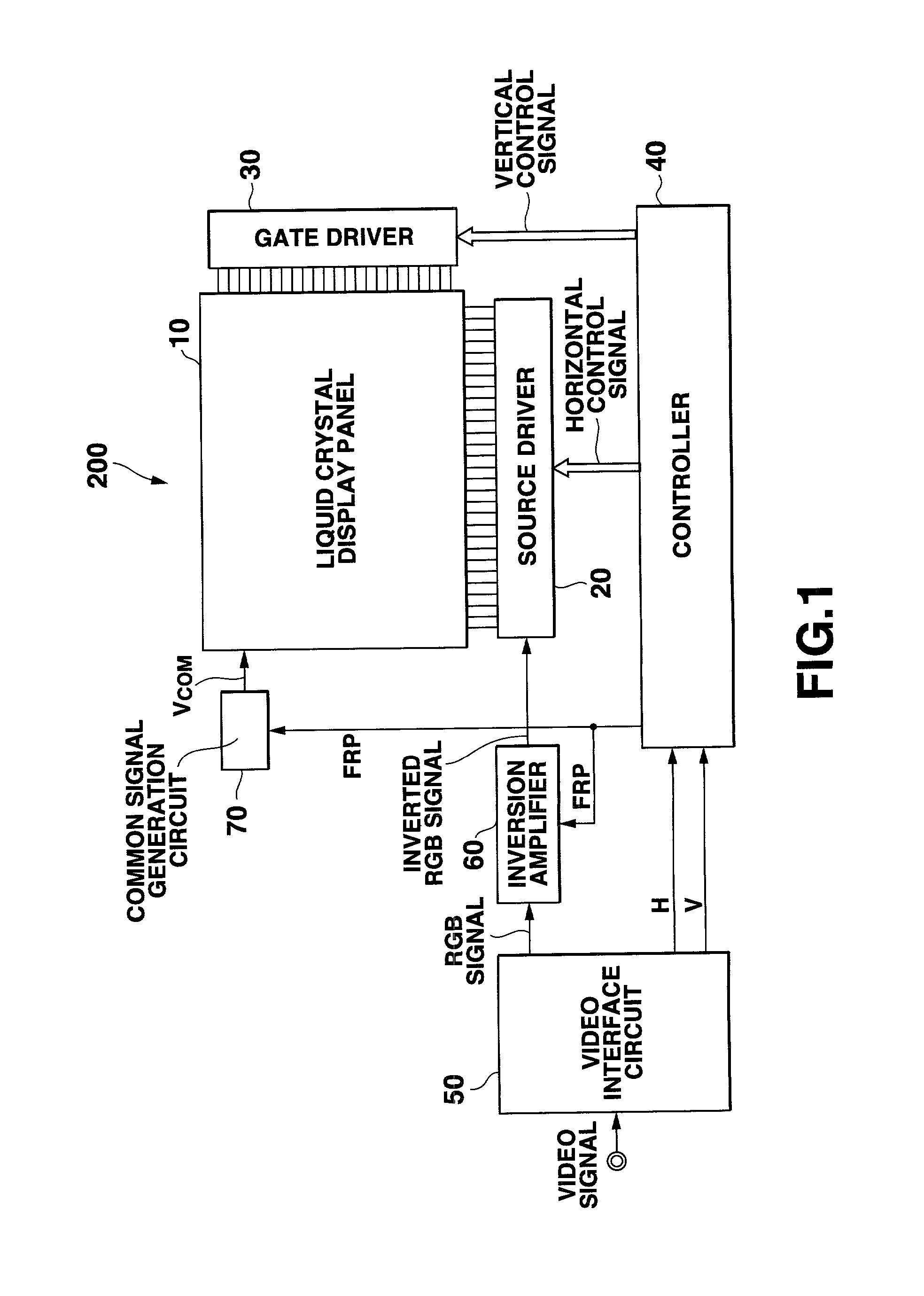
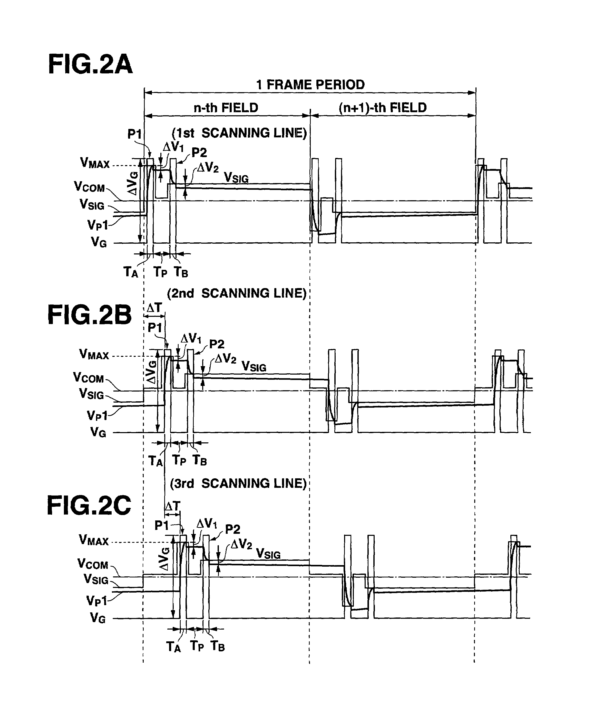
[0038]FIG. 1 is a block diagram showing a structural example of a liquid crystal display device according to the first embodiment of the present invention. For conveniences, explanation will be made appropriately referring to the structure of a liquid crystal display panel 100 shown in FIG. 8A.

[0039]As shown in FIG. 1, a liquid crystal display device 200 has a liquid crystal display panel 10, a source driver 20, a gate driver 30, a controller 40, a video interface circuit 50, an inversion amplifier 60, and a common signal generation circuit 70, where it is roughly classified.

[0040]The structure of each component will now be explained.

[0041]The liquid crystal display panel 10 comprises a plurality of scanning lines GL extended in the row direction of the liquid crystal display panel, a plurality of signal lines DL extended in the column direction, pixel transistors TFT provided respectively near the cross-points between the signal lines DL and the scanning lines GL, pixel electrodes ...

second embodiment

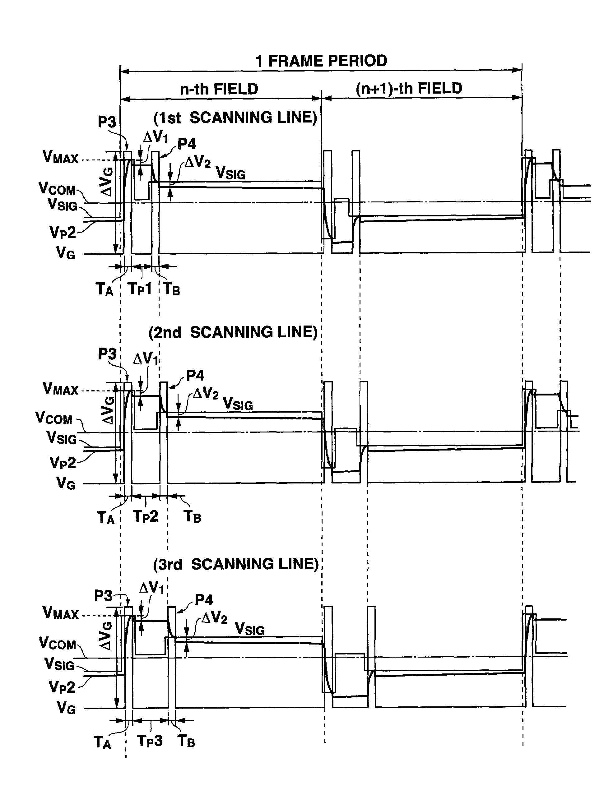
[0077]Next, a drive control method according to the second embodiment of a liquid crystal display device according to the present invention will be explained with reference to the drawings. The structure of the liquid crystal display device is the same as that of the liquid crystal display device 200 shown in FIG. 1. Explanation will now be made with reference to the structure of the liquid crystal display device 200 shown in FIG. 1 and the structure of the liquid crystal display panel 100 shown in FIG. 8A. Operations that are equivalent to those of the first embodiment described above will be explained with use of equal reference symbols.

[0078]The drive control method for the liquid crystal display device according to the present embodiment is characterized in that the black signal voltage Vmax described previously is applied simultaneously to all the display pixels of the liquid crystal display panel, at first, and thereafter, the display signal voltage Vsig is sequentially applie...

third embodiment

[0096]Next, the structure of a liquid crystal display device according to the third embodiment of the present invention and the drive control method thereof will be explained with reference to the drawings.

[0097]The first and second embodiments described above are structured such that the signal application period is set as one field period and the screen is overwritten for every one field period. In the third embodiment, however, one field period comprises three sub-field periods, and each of the sub-field periods corresponds to the signal application period in the embodiments described above. The present embodiment is characterized in that the sub-fields are set as periods for displaying red, green, and blue components of a video signal, and a drive control method similar to the second embodiment is adopted to perform field-sequential driving.

[0098]FIG. 6 is a block diagram showing a structural example of a liquid crystal display device according to the third embodiment of the pre...


PUM

PropertyMeasurementUnit
response timeaaaaaaaaaa
hold time Tpaaaaaaaaaa
response timeaaaaaaaaaa

Abstract

In a liquid crystal display device of an active matrix type, at first, an initialization signal voltage having a voltage value equal to or higher than the maximum voltage value of a display signal is applied to display pixels in a signal application period in a field period. The display signal is thereafter applied. As a result, the change amount of the voltage applied to liquid crystal due to the field-through voltage in relation to a gate pulse can be arranged to be substantially constant, and can always be cancelled by a common electrode voltage. Occurrence of flicker and seizure phenomena can be thereby restricted so that the display quality can be improved.

Description

CROSS-REFERENCE TO RELATED APPLICATIONS[0001]This application is based upon and claims the benefit of priority from the prior Japanese Patent Application No. 2000-343926, filed Nov. 10, 2000, the entire contents of which are incorporated herein by reference.BACKGROUND OF THE INVENTION[0002]1. Field of the Invention[0003]The present invention relates to a liquid crystal display device and a driving control method thereof, and particularly to a liquid crystal display device of an active matrix type which uses a plurality of thin-film transistors as switching elements, and a driving control method thereof.[0004]2. Description of the Related Art[0005]In recent years, liquid crystal display devices (LCD) for displaying images, text information, and the like are mounted on image pickup apparatuses represented by digital video cameras, digital still cameras, and the like, portable phones, and personal digital assistants (PDA). Further, in place of conventional cathode ray tubes (CRTs), liq...

Claims


Application Information

Patent Timeline
Patent Type & Authority Patents(United States)
IPC IPC(8): G09G3/36G02F1/133G09G3/20
CPCG09G3/3648G09G3/3614G09G3/3655G09G2320/0219G09G3/36
Inventor SHIMOMAKI, SHINICHI
Owner CASIO COMPUTER CO LTD
Why Eureka
Try Eureka