Timing analysis method and apparatus
a timing analysis and time-based technology, applied in the field of timing analysis methods and apparatuses, can solve the problems of difficult to determine the appropriate design margin, inability to take into account intra-chip variation, etc., and achieve the effects of avoiding excessive margins, and realistic and highly accurate timing design
- Summary
- Abstract
- Description
- Claims
- Application Information
AI Technical Summary
Benefits of technology
Problems solved by technology
Method used
Image
Examples
embodiment 1
[0073]Now, a timing analysis apparatus for an LSI according to Embodiment 1 of the invention in which fabrication variation is taken into consideration will be described with reference to the accompanying drawings.
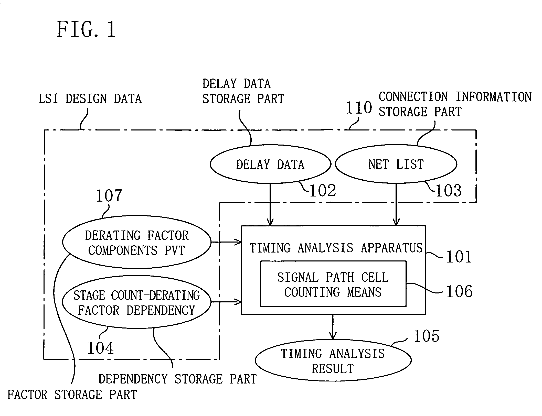
[0074]FIG. 1 is a block diagram for showing the architecture of a system used for performing the timing analysis for an LSI according to Embodiment 1 of the invention. As shown in FIG. 1, a timing analysis apparatus 101 performs the timing analysis on the basis of information supplied from respective information storage parts of LSI design data 110 in which information on the LSI is comprehensively stored. The LSI design data 110 includes a connection information storage part for storing a net list 103 describing connection information and the like of circuit cells included in the LSI; a delay information storage part for previously storing delay data 102 describing delay information of the circuit cells; a dependency storage part for storing stage count-derating factor de...
modification 1
of Embodiment 1
[0108]FIG. 11 is a block diagram of a signal path used in Modification 1 of Embodiment 1. In the timing analysis method in consideration of the fabrication variation of Embodiment 1, the two flip-flops 211 and 212 delimiting the one signal path 200 receive a clock signal from the one clock output terminal 201 as shown in FIG. 3.
[0109]However, a clock signal supply circuit frequently has a clock tree structure that is successively branched from the root thereof.
[0110]Therefore, in Modification 1 shown in FIG. 11, clock terminals CLK of two flip-flops 211 and 212 delimiting a signal path 200 are respectively connected to clock output terminals disposed at the tips of two clock signal paths 252 and 253 of a clock signal supply circuit 250. It is assumed that the same number of buffers are disposed on the two clock signal paths 252 and 253 extending from an input terminal 251 of the clock signal supply circuit 250 to the clock output terminals at the tips. Also in this ca...
modification 2
of Embodiment 1
[0112]Furthermore, in the case where an LSI is designed by using a plurality of hierarchies, a signal path may extend over a plurality of circuit blocks. In this case, it is necessary to count the number of stages disposed from the entrance to the exit of a signal path sandwiched between two flip-flops respectively present in different circuit blocks.
[0113]FIG. 12 is a block diagram for showing the structure of a circuit to be analyzed in Modification 2 of Embodiment 1. As shown in FIG. 12, in this modification, a chip 271 includes circuit blocks 272 and 273, and a signal path 275 starting from a flip-flop 276 disposed in the circuit block 273 extends to a flip-flop 277 disposed in the circuit block 272. In other words, the signal path 275 includes circuit cells 274 disposed in the plural circuit blocks 272 and 273. In this case, the stage count of the signal path 275 is three stages in the circuit block 273 and four stages in the circuit block 272, namely, seven stag...
PUM
 Abstract
Description
Claims
Application Information


