Printed wiring board and method of fabricating the same

a technology of printed wiring boards and wires, which is applied in the manufacture of printed circuit boards, printed circuit assembling, lamination printed circuit boards, etc., can solve the problems of thickness exceeding the maximum allowable value of some products, and achieve the effect of reducing thickness

Active Publication Date: 2007-05-29
SUBTRON TECH
View PDF1 Cites 36 Cited by
  • Summary
  • Abstract
  • Description
  • Claims
  • Application Information

AI Technical Summary

Benefits of technology

[0013]A third purpose of the present invention is to provide a printed wiring board with reduced thickness.

Problems solved by technology

However, the core layer has a definite thickness which, together with the build up layers on both sides, may result in a thickness exceeding the maximal allowable value required by some products.

Method used


Image

  • Printed wiring board and method of fabricating the same
  • Printed wiring board and method of fabricating the same
  • Printed wiring board and method of fabricating the same

Examples


first embodiment

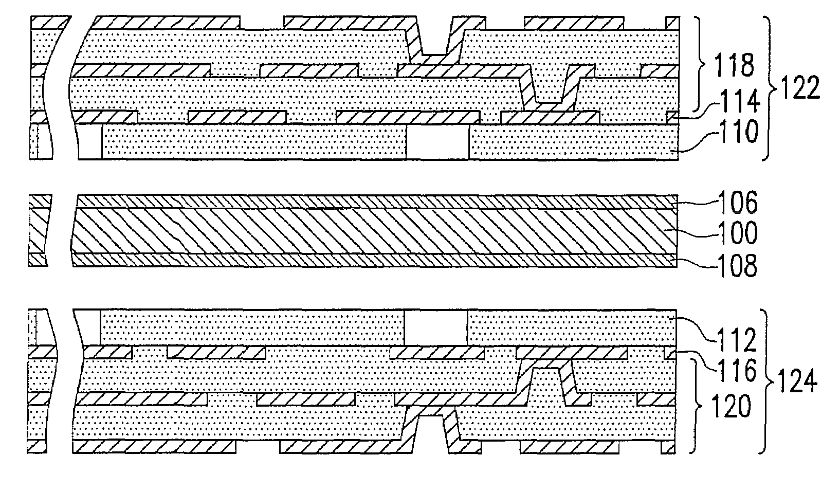
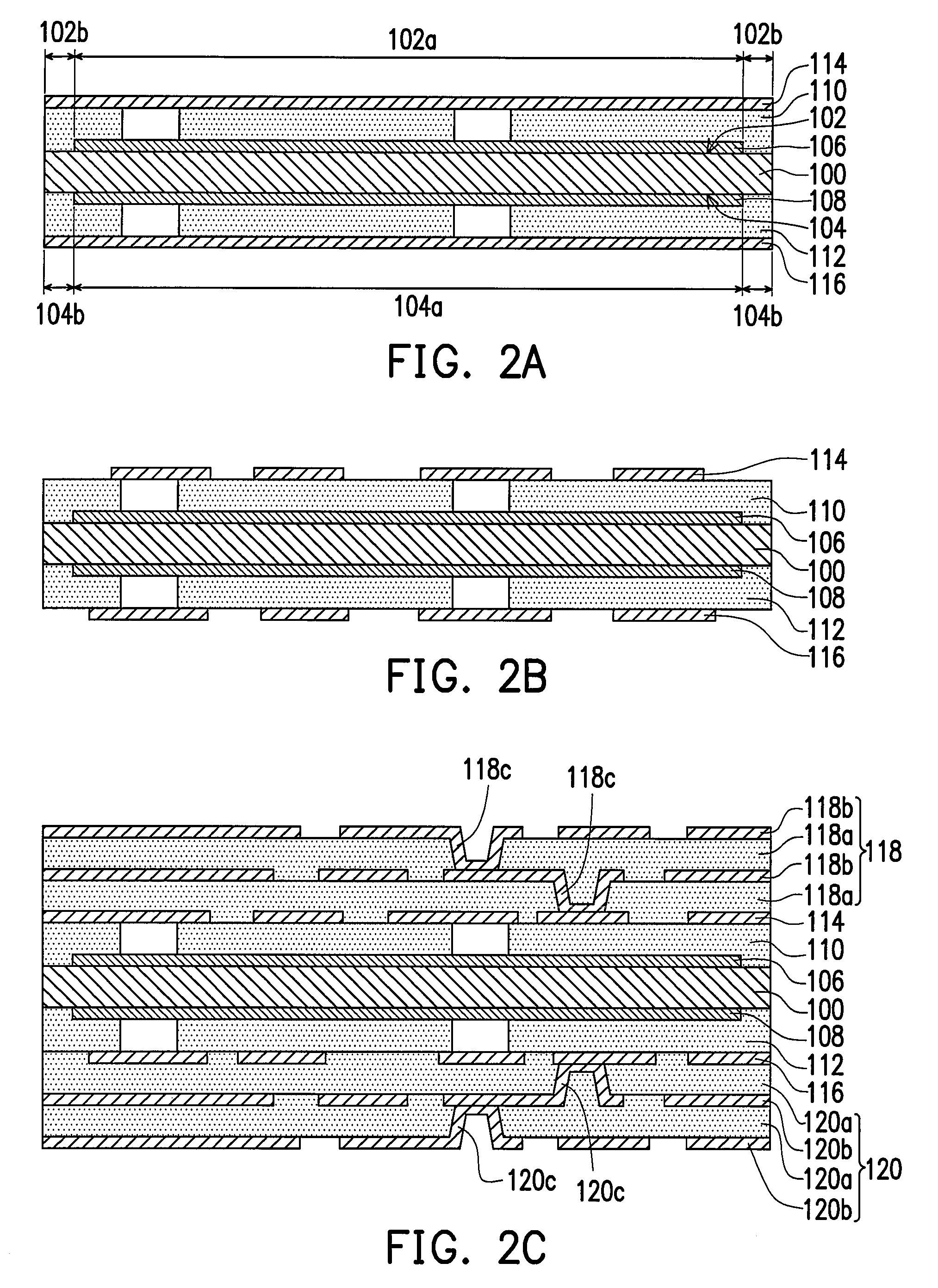
[0026]FIGS. 2A to 2E are schematic, cross-sectional diagrams illustrating the process steps for fabricating a printed wiring board according to the present invention. Referring to FIG. 2A, first, a carrier plate 100 having a first supporting surface 102 and a second supporting surface 104 opposite to the first supporting surface 102 is provided. The first supporting surface 102 has a first release region 102a and a first bonding region 102b, and the second supporting surface 104 has a second release region 104a and a second bonding region 104b. The carrier plate 100 may be a thin metal plate such as copper plate.

[0027]As shown in FIG. 2A, a first release layer 106 and a second release layer 108 are arranged on the first release region 102a and the second release region 104a, respectively. In the first embodiment, a material of the first release layer 106 and the second release layer 108 may comprise dielectric material such as polyethylene terephthalate (PET).

[0028]As shown in FIG. ...

second embodiment

[0035]As shown in FIG. 3A, a first conductive layer 206 and a second conductive layer 208 are arranged on the first release region 202a and the second release region 204a, respectively. Wherein, a surface of the first conductive layer 206, which faces the first release region 202a of the carrier plate 200, has temporary adhesion; a surface of the second conductive layer 208, which faces the second release region 204a of the carrier plate 200, has temporary adhesion. In the second embodiment, the first conductive layer 206 and the second conductive layer 208 may be comprised of a metal such as copper.

[0036]As shown in FIG. 3A, a first dielectric layer 210 and a second dielectric layer 212 are arranged on the first supporting surface 202 and the second supporting surface 204, respectively, and a third conductive layer 214 and a fourth conductive layer 216 are arranged on the first dielectric layer 210 and the second dielectric layer 212, respectively. Next, a portion of the first diel...


PUM

PropertyMeasurementUnit
conductiveaaaaaaaaaa
bonding forceaaaaaaaaaa
dielectricaaaaaaaaaa

Abstract

A method of fabricating a printed wiring board comprising the following steps is provided. A portion of each of two dielectric layers or metal layers bonds to both sides of a carrier plate, respectively. Two build-up wiring structures are respectively formed on the dielectric layers or the metal layers by a build-up process. The portions of the dielectric layers or metal layers bonded to the carrier plate are removed such that the dielectric layers or metal layers and the build-up wiring structures formed thereon are released from the carrier plate to form two printed wiring boards.

Description

CROSS-REFERENCE TO RELATED APPLICATION[0001]This application claims the priority benefit of Taiwan application serial no. 94147149, filed on Dec. 29, 2005. All disclosure of the Taiwan application is incorporated herein by reference.BACKGROUND OF THE INVENTION[0002]1. Field of the Invention[0003]The present invention generally relates to a printed wiring board, and more particularly, to a printed wiring board and method of fabricating the same.[0004]2. Description of Related Art[0005]The common printed wiring board is usually fabricated by lamination or build-up process. In the conventional lamination process, a predetermined number of the single-sided boards or the double-sided boards are provided. Wherein, the single-sided board means that a dielectric layer has a single conductive layer formed thereon, and the double-sided board means that a dielectric layer has two conductive layers formed on its two surfaces thereof respectively. Next, the conductive layers of the single-sided ...

Claims


Application Information

Patent Timeline
Patent Type & Authority Patents(United States)
IPC IPC(8): H01L21/4763
CPCH05K3/0058H05K3/4682H05K3/0097Y10T29/49126H05K2203/1536Y10T29/49124H05K2203/0152
Inventor HO, CHUNG W.CHENG, SHIH-LIANSHEN, LEO
Owner SUBTRON TECH
Why Eureka
Try Eureka