AI technical title is built by Patsnap AI team. It summarizes the technical point description of the patent document.
a maskless lithography and maskless technology, applied in the field of maskless lithography, can solve the problems of significant number and complexity of processing steps presently used, and achieve the effects of reducing cost and process complexity, superior mechanical handling properties, and inexpensive and well-known
Inactive Publication Date: 2007-05-29
TAIWAN SEMICON MFG CO LTD
View PDF255 Cites 19 Cited by
Summary
Abstract
Description
Claims
Application Information
AI Technical Summary
This helps you quickly interpret patents by identifying the three key elements:
Problems solved by technology
Method used
Benefits of technology
Benefits of technology
[0012]The primary objectives of the MDI fabrication technology disclosed herein are the cost effective manufacture of high performance, high density integrated circuits and integrated circuit interconnect with the elimination or reduction of detrimental electrical effects on the operation of individual circuit devices (e.g. diodes, transistors, etc.) by completely isolating with a dielectric material each such circuit device from the common substrate upon which they are initially fabricated, and therefore, from each other, and to provide a more versatile and efficient physical form factor for the application of integrate circuits. Some of the benefits of the MDI IC fabrication process are the elimination or reduction of substrate current leakage, capacitive coupling and parasitic transistor effects between adjoining circuit devices. The MDI IC fabrication process benefits extend to several other categories of IC fabrication such as lower IC processing costs due to fewer IC isolation processing steps, greater IC transistor densities through the capability to use established IC processing techniques to fabricate interconnect metallization on both sides of a MDI IC circuit membrane, and greater IC performance through novel transistor structures.
[0025]3. Lower processing costs through lower processing complexity or fewer device isolation processing steps.
Problems solved by technology
ICs formed from dielectric and semiconductor membranes can reduce significantly the number and complexity of processing steps presently used to provide complete IC device isolation; dielectric isolation techniques that provide dielectric isolation on all surfaces of the individual circuit devices comprising the complete IC are not as yet widely used in volume IC fabrication.
Method used
Image
Click on the blue label to locate the original text in one second.
Reading with bidirectional positioning of images and text.
Examples
Embodiment Construction
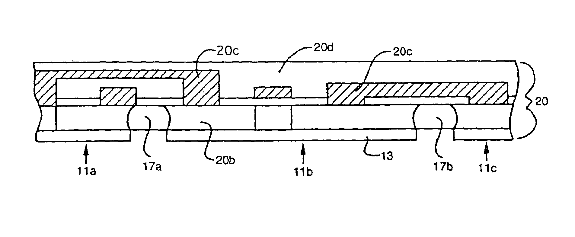
[0069]The MDI process is the formation of an IC or interconnect metallization circuit as a free standing dielectric and / or semiconductor circuit membrane. Each semiconductor device comprising an IC circuit membrane is a semiconductor device optionally isolated from adjoining semiconductor devices, and where each semiconductor device is formed on or in a membrane of semiconductor material typically less than 8 μm in thickness. The overall thickness of a circuit membrane is typically less than 50 μm and preferably less than 8 μm. The dielectric membrane is compatible with most higher temperature IC processing techniques.
MDI Fabrication Process
[0070]Several process variations can be used to form the thin film or membrane of semiconductor material for use in the MDI process. Additional related methods for forming semiconductor membranes may exist or come into existence and are included in the MDI technology.
[0071]Examples of some of the methods that can be used for forming silicon singl...
PUM
Property
Measurement
Unit
area
aaaaa
aaaaa
processing temperatures
aaaaa
aaaaa
width
aaaaa
aaaaa
Abstract
General purpose methods for the fabrication of integrated circuits from flexible membranes formed of very thin low stress dielectric materials, such as silicon dioxide or silicon nitride, and semiconductor layers. Semiconductor devices are formed in a semiconductor layer of the membrane. The semiconductor membrane layer is initially formed from a substrate of standard thickness, and all but a thin surface layer of the substrate is then etched or polished away. In another version, the flexible membrane is used as support and electrical interconnect for conventional integrated circuit die bonded thereto, with the interconnect formed in multiple layers in the membrane. Multiple die can be connected to one such membrane, which is then packaged as a multi-chip module. Other applications are based on (circuit) membrane processing for bipolar and MOSFET transistor fabrication, low impedance conductor interconnecting fabrication, flat panel displays, maskless (direct write) lithography, and 3D IC fabrication.
Description
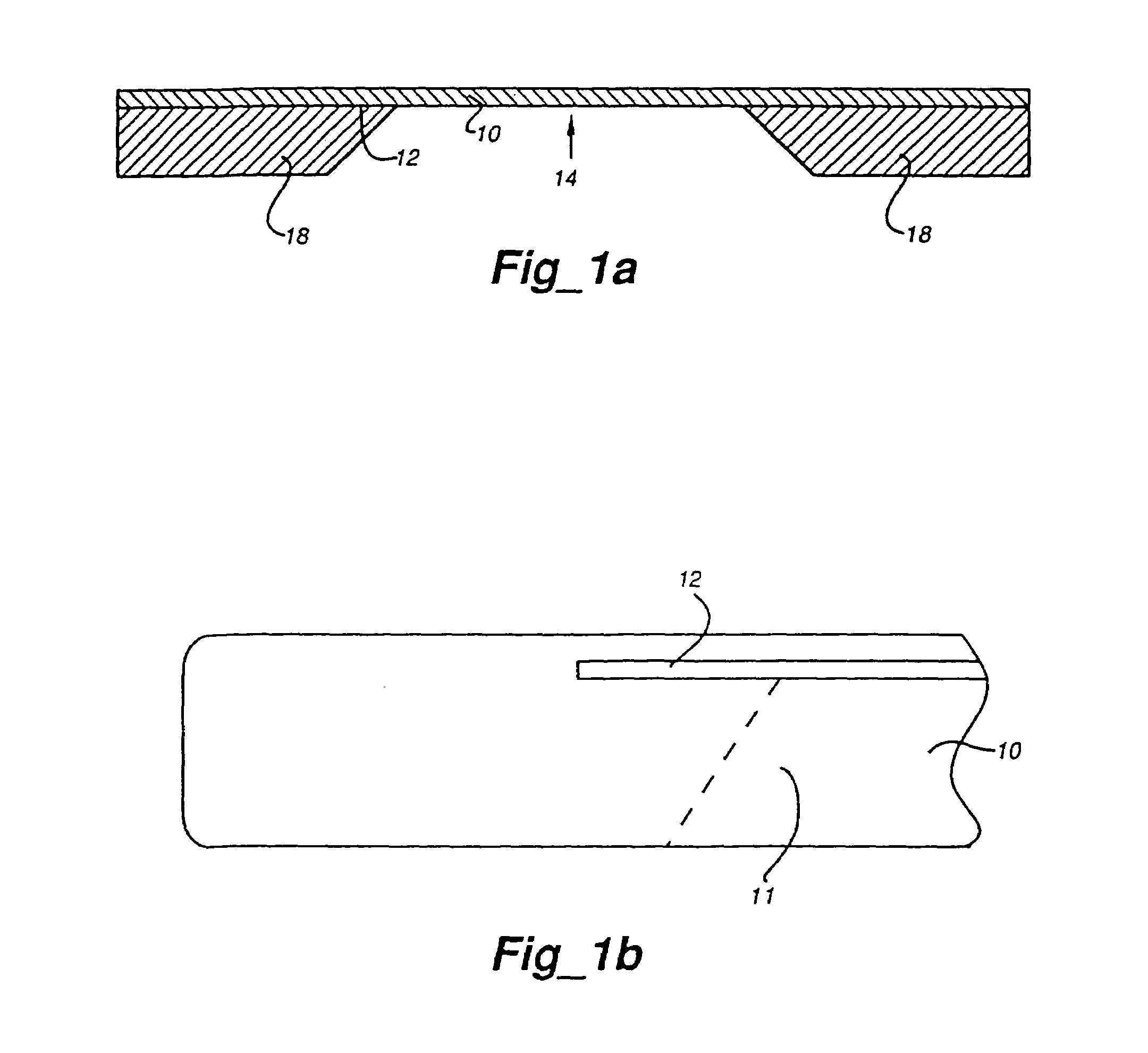
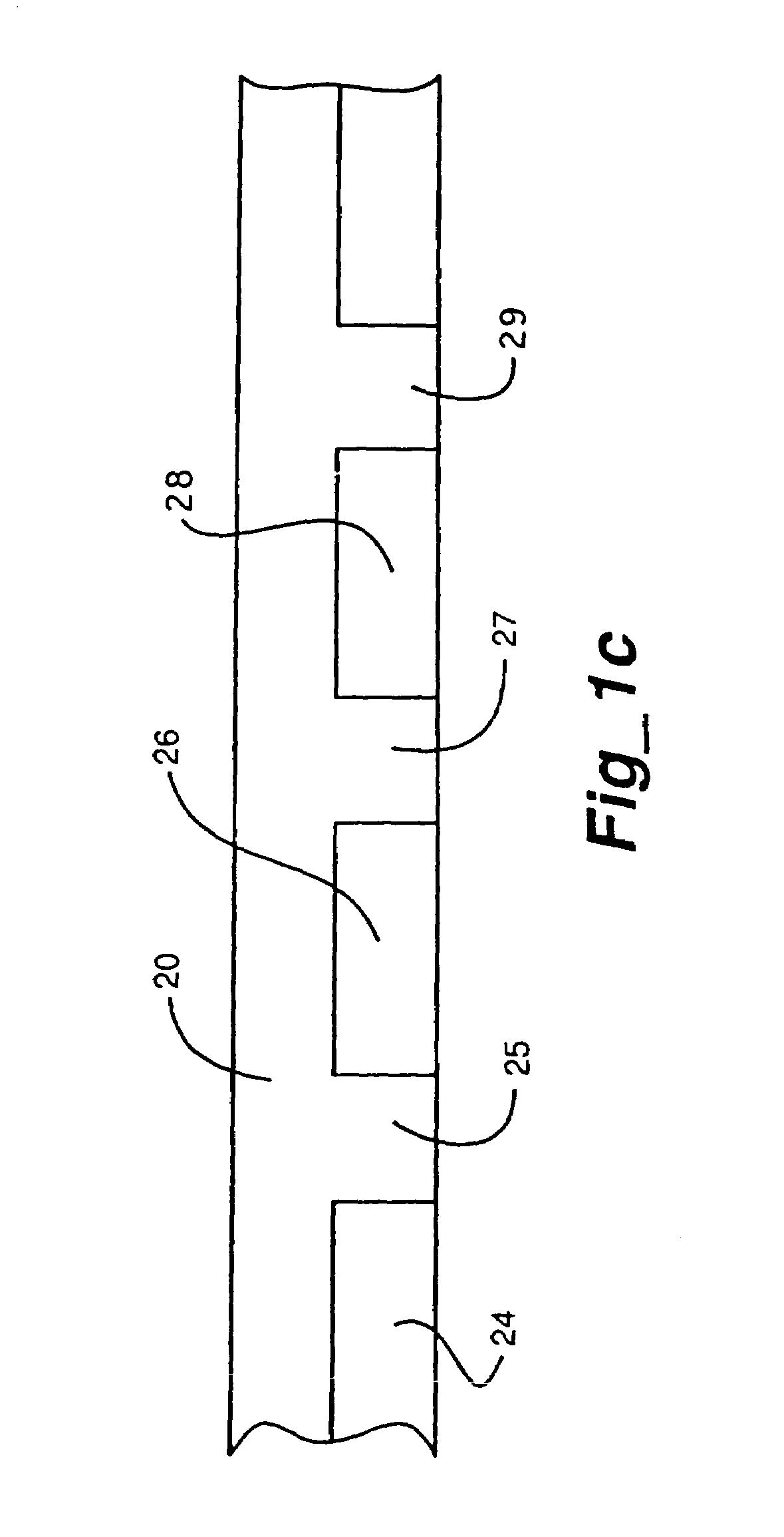
CROSS REFERENCE TO RELATED APPLICATIONS[0001]This application is a continuation of commonly assigned U.S. patent application Ser. No. 08 / 483,731, filed Jun. 7, 1995 now U.S. Pat. No. 6,714,625, which is a continuation of U.S. patent application Ser. No. 08 / 315,905, filed Sep. 30, 1994, now U.S. Pat. No. 5,869,354, which is a division of U.S. patent application Ser. No. 07 / 865,412, filed Apr. 8, 1992, now U.S. Pat. No. 5,354,695, all of which are incorporated by reference herein in their entireties.BACKGROUND OF THE INVENTION[0002]1. Field of the Invention[0003]This invention relates to methods for fabricating integrated circuits on and in flexible membranes, and to structures fabricated using such methods.[0004]2. Description of Related Art[0005]Mechanically and thermally durable free standing dielectric and semiconductor membranes have been disclosed with thicknesses of less than 2 μm. (See commonly invented U.S. Pat. No. 4,924,589, and U.S. patent application Ser. No. 07 / 482,135, ...
Claims
Application Information
Patent Timeline
Application Date:The date an application was filed.
Publication Date:The date a patent or application was officially published.
First Publication Date:The earliest publication date of a patent with the same application number.
Issue Date:Publication date of the patent grant document.
PCT Entry Date:The Entry date of PCT National Phase.
Estimated Expiry Date:The statutory expiry date of a patent right according to the Patent Law, and it is the longest term of protection that the patent right can achieve without the termination of the patent right due to other reasons(Term extension factor has been taken into account ).
Invalid Date:Actual expiry date is based on effective date or publication date of legal transaction data of invalid patent.

