Method for producing a fluid device, fluid device and analysis apparatus

a fluid device and analysis apparatus technology, applied in the field of analytical methods, can solve the problems of increasing the cost of the fluid device, difficult to adjust the precise depth of the fluid structure by means of etching methods, and inconvenient capillary paths for transmitted light analysis, etc., to achieve the effect of reducing the production cost per fluid device, high accuracy and precise active height of the fluid structur

Inactive Publication Date: 2007-06-05
FEBIT HOLDING GMBH +1
View PDF7 Cites 53 Cited by
  • Summary
  • Abstract
  • Description
  • Claims
  • Application Information

AI Technical Summary

Benefits of technology

[0017]One advantage of the present invention is that a fluid device which is transparent on both sides has now been created, which can easily be used for transmitted-light analyses.
[0018]A further advantage of the present invention is that it is no longer necessary to adjust the active height of the fluid structure by very precisely controlled etching parameters, this height being simply determined by the thickness of the semiconductor layer. The accuracy of the active height of the fluid structure is therefore already determined prior to the actual production of the fluid device, viz. by the thickness of the semiconductor layer specified by the manufacturer of the basic wafer.
[0019]A further advantage of the present invention is that, during the patterning of the semiconductor layer, etching methods can be used, which need not be controlled precisely. On the contrary, the insulating layer of the basic wafer automatically acts as an etch stop so that a very precise active height of the fluid structure will always be achieved independently of the etching parameters. The only requirement to be satisfied is that the semiconductor layer is fully etched through so as to achieve a fluid structure having a constant height.
[0020]Still another advantage of the present invention is that fluid devices for many different cases of use, i.e. with many different respective active heights of the fluid structures, can be obtained by means of the same production method by simply selecting different basic wafers with different thicknesses of the semiconductor layers. Since the same production method can therefore be used for a large number of different fluid devices, the production costs per fluid device will be reduced because even small batches of fluid devices having different specifications can be produced, without any complicated change-over of the production plant being necessary after each small batch.
[0021]All this is achieved due to the fact that the decisive parameter, viz. the active height of the fluid structure, is no longer determined by the production process itself, but by the starting material, viz. the basic wafer.
[0022]It follows that according to the present invention fluid devices closed on both sides thereof with transparent wafers, e.g. glass covers, can be produced with high accuracy. The accuracy is no longer-determined by the production method, but by the use of basic wafers. Due to the fact that the fluid structures are obtained by standard semiconductor-technology process steps, it is also possible to produce very complicated fluid structures with arbitrary geometries on a basic wafer so that the method according to the present invention can be used for producing not only capillary paths but also cavities, branches, passive valves and the like.

Problems solved by technology

Hence, such capillary paths are not suitable for transmitted-light analyses.
In addition to the fact that such capillary paths are not suitable for transmitted-light determinations, the application of a mirror coating to the silicon is a further production step, which is complicated and which increases the costs for the fluid device.
In addition, it is difficult to adjust precise depths of the fluid structure by means of etching methods.
It is true that very precisely controllable amounts of material can be removed by dry-etching techniques, but these techniques are disadvantageous insofar as the etching parameters must be controlled very precisely; this, in turn, results in high production costs for such capillary components.
If the etching parameters are not strictly controlled in this way, a high reject rate will occur in the production process.

Method used


Image

  • Method for producing a fluid device, fluid device and analysis apparatus
  • Method for producing a fluid device, fluid device and analysis apparatus

Examples


Embodiment Construction

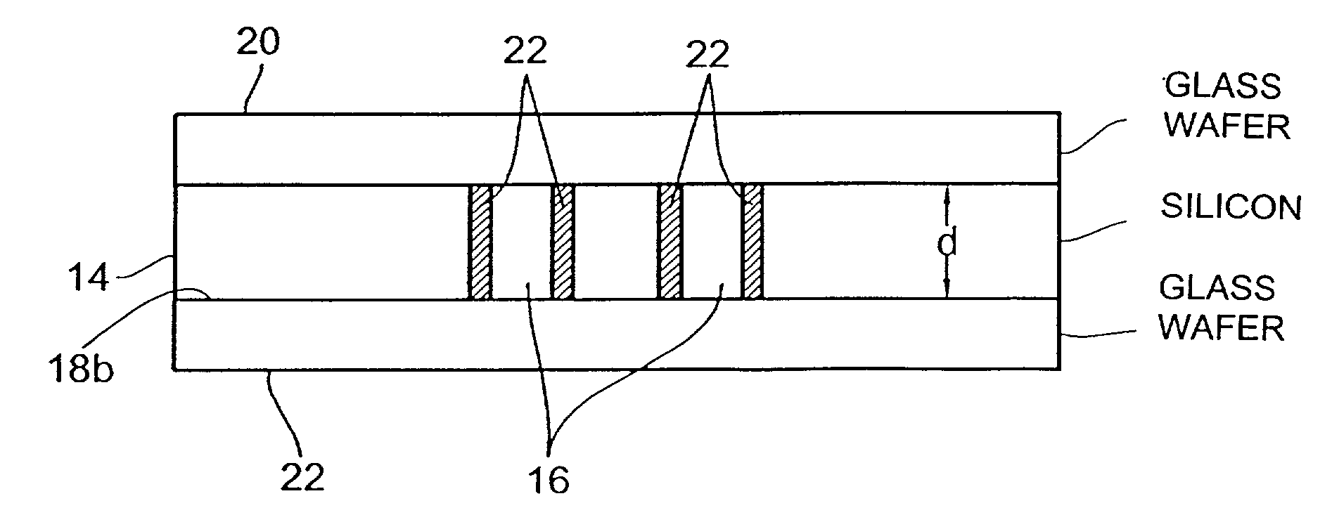
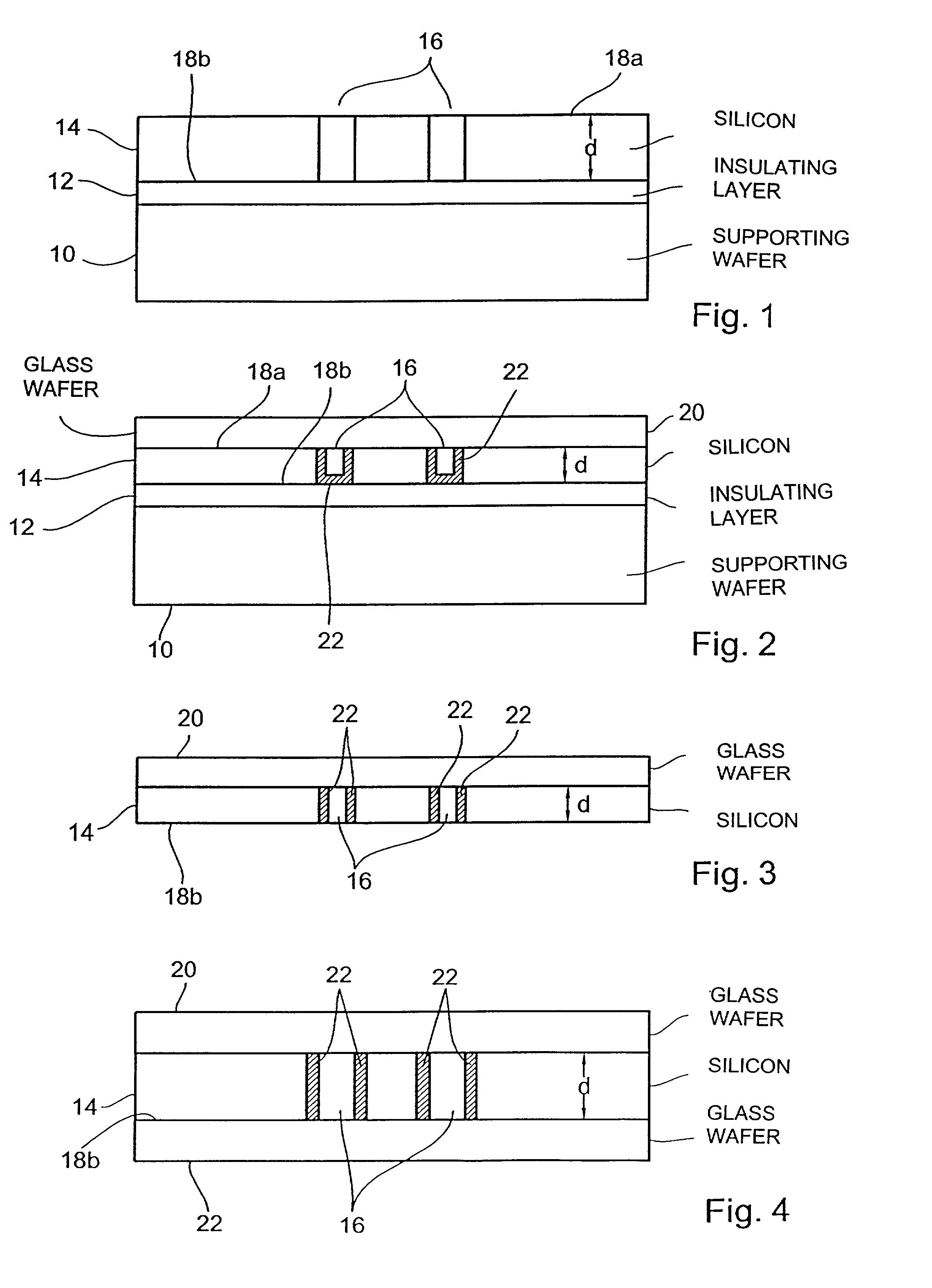
[0028]FIG. 1 shows a basic wafer comprising a supporting wafer 10 having applied thereto an insulating layer 12 which is, in turn, covered by a semiconductor layer 14. An SOI structure is preferably used as a basic wafer, i.e. a structure in the case of which the semiconductor layer consists of silicon, the insulating layer consists of silicon oxide, and also the supporting wafer 10 is produced from silicon. In FIG. 1, a fluid structure 16 is already shown, which is preferably produced by dry etching the silicon layer 14. As known in the field of technology, a photoresist is applied to the semiconductor layer prior to the dry-etching step; this photoresist is then exposed at the locations at which the fluid structure 16 is to be created.

[0029]The present invention is also applicable to all supporting-structure / intermediate-layer / patterned-layer systems in the case of which the intermediate layer is of such a nature that it is essentially not impaired by a patterning process used for...


PUM

PropertyMeasurementUnit
heightaaaaaaaaaa
thicknessaaaaaaaaaa
transparentaaaaaaaaaa

Abstract

In the case of a method for producing a fluid device with a fluid structure having an active height, a basic wafer is provided, which comprises a supporting substrate, an insulating layer on the supporting substrate and a patterned layer on the supporting substrate, the thickness of the patterned layer determining the active height of the fluid structure. Following this, the fluid structure is produced in the patterned layer of the basic wafer, said fluid structure extending through the semiconductor layer. A transparent wafer is then applied so that the fluid structure is covered. Subsequently, the supporting substrate and the insulating layer are removed from the back so that the fluid structure is exposed at a second surface of the patterned layer. Finally, a second transparent wafer is attached to the exposed second surface of the semiconductor layer so that the fluid structure is covered. The essential parameter of the fluid device, viz. the active height of the fluid structure, need no longer be controlled making use of the etching parameters, but is already determined by the specifications of the starting material, e.g. an SOI wafer. This means that economy-priced fluid devices can be produced with high precision.

Description

FIELD OF THE INVENTION[0001]The present invention relates to analytics and in particular to fluid devices which are suitable for analytic applications.BACKGROUND OF THE INVENTION AND PRIOR ART[0002]In the field of analytics there is a great demand for fluid devices and in particular capillary paths for transporting e.g. fluids by means of capillary forces, for examining them while they are being transported or for producing sample receptacles in which the fluids stand and the surfaces of which are treated with chemical substances so that specific sample fluids will undergo a reaction with these substances, said reaction causing e.g. a change in colour of these sample fluids. In order to be able to detect such a change in colour of a sample fluid, or in order to be able to detect the optical properties of a sample fluid in general, it is important that fluid devices are transparent on both sides so that analyses can be carried out in transmitted light, e.g. by making use of fluoresce...

Claims


Application Information

Patent Timeline
Patent Type & Authority Patents(United States)
IPC IPC(8): H01L21/302B01L3/02H01L21/20H01L21/36H01L21/461B01L3/00B01L99/00B81B1/00B81C1/00
CPCB01L3/502707B81B1/00B81C1/00357B81C1/00119B01L2200/12B81B2201/058B81B2203/0338Y10T436/25B81C2201/019Y10T436/2575Y10T436/11
Inventor STAEHLER, CORD F.STROBELT, TILOFRECH, JOHANNESNOMMENSEN, PETERMUELLER, MARTIN
Owner FEBIT HOLDING GMBH
Why Eureka
Try Eureka