Supercharge Your Innovation With Domain-Expert AI Agents!

Address latch signal generation circuit and address decoding circuit

a signal generation circuit and address technology, applied in the direction of information storage, static storage, digital storage, etc., can solve the problems of i/o associated errors, inapplicability of methods to timing adjustment processes, and ineffective above-mentioned conventional methods, so as to prevent i/o-associated errors and prevent skews or glitches

Active Publication Date: 2007-06-05
SK HYNIX INC
View PDF7 Cites 13 Cited by
  • Summary
  • Abstract
  • Description
  • Claims
  • Application Information

AI Technical Summary

Benefits of technology

The patent describes an address latch signal generation circuit and an address decoding circuit that can prevent errors and ensure proper timing when accessing internal address signals. The circuit includes multiple address transition detectors that detect level transitions in the internal address signals and generate control signals with a predetermined enable period. A logic unit performs logic operations on the control signals and generates the result signal. A latch signal output unit synchronizes with the result signal and generates the address latch signal. The address latch signal generation circuit can prevent skew or glitches and prevent I / O-related errors. The address decoding circuit can accurately select the desired column and prevent errors in accessing the internal address signals.

Problems solved by technology

However, as shown in a reference number “304” in FIG. 3, if the latch signal YAEDI is enabled without guaranteeing a sufficient timing margin associated with level-transition time points of the internal column address signals AY0H0:7>, AY3H0:7>, and AY6H0:3> applied to the Y-address latch unit 106, the Y-address latch 106 cannot perform a normal latch operation, resulting in the occurrence of I / O associated errors such as the selection of two-cells, etc.
In this case, if the time margin is sufficiently guaranteed as shown in 302 or 304 of FIG. 3, the glitch is not removed, and two column selection signals are finally generated, such that there arises an unexpected error in which two cells are simultaneously selected from a memory core.
The above-mentioned conventional method for controlling the enable time point of the address latch signal YAEDI using fuses can be executed in a wafer stage, and the fuses cannot be severed in a package stage, such that the above-mentioned conventional method is not applicable to a timing adjusting process.
Furthermore, although a semiconductor successfully passes a memory test process, it may unexpectedly generate an error in a mounting application stage, such that the above-mentioned conventional method is useless in the above-mentioned case.

Method used


Image

  • Address latch signal generation circuit and address decoding circuit
  • Address latch signal generation circuit and address decoding circuit
  • Address latch signal generation circuit and address decoding circuit

Examples


Embodiment Construction

[0038]Now, various embodiments of the present invention will be described with reference to the annexed drawings. In the drawings, the same or similar elements are denoted by the same reference numerals even though they are depicted in different drawings. In the following description, a detailed description of known functions and configurations is omitted.

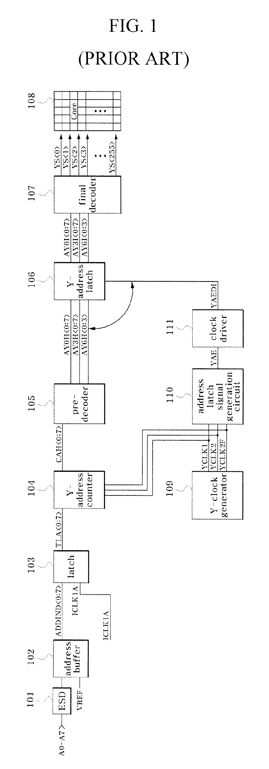
[0039]FIG. 5 is a block diagram illustrating a column address path of a semiconductor device according to one or more of the herein described embodiments.

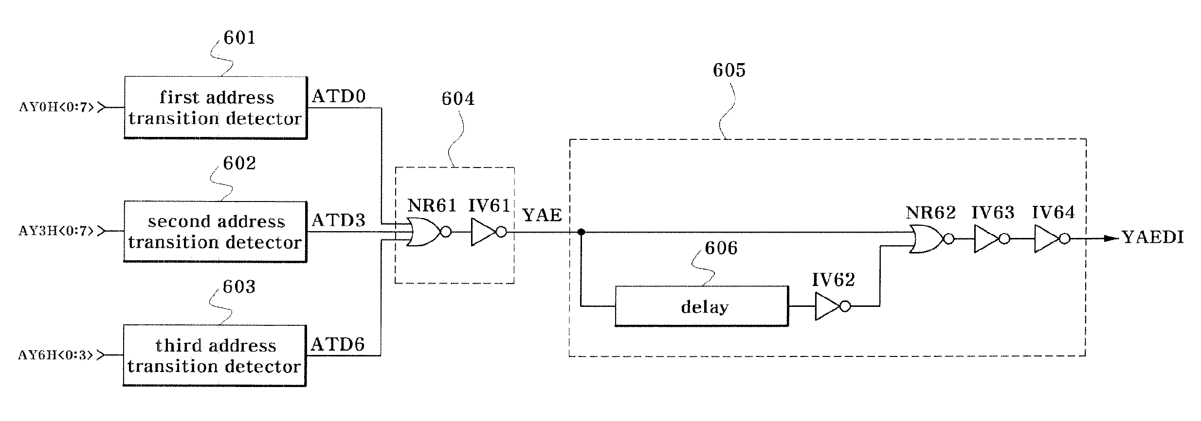
[0040]FIG. 6 is a block diagram illustrating an address latch signal generation circuit in accordance with one or more of the herein described embodiments. FIG. 7 is a circuit diagram illustrating an address transition detector for use in an address latch signal generation circuit in accordance with one or more of the herein described embodiments.

[0041]Referring to FIG. 5, the address latch signal generation circuit may include a plurality of address transition detectors 601˜603, ...


PUM


Abstract

An address latch signal generation circuit and an address decoding circuit may generate an address latch signal capable of latching pre-decoded internal address signals. The circuits may include a plurality of address transition detectors, each of the address transition detectors receiving a plurality of internal address signals pre-decoded by a pre-decoder, detecting level transition states of the internal address signals, and generating a control signal which has a predetermined enable period; a first logic unit for performing a logic operation on the control signals received from the plurality of address transition detectors, and generating the result signal; and a latch signal output unit for performing synchronization with a disable time point of the result signal from the first logic unit, thereby generating the address latch signal.

Description

FIELD OF THE INVENTION[0001]The present invention relates to an address latch signal generation circuit and an address decoding circuit using the same, and more particularly to an address latch signal generation circuit for generating an address latch signal to latch a pre-decoded internal column address signal, and an address decoding circuit using the same.DESCRIPTION OF THE RELATED ART[0002]In the case of an active cycle of a semiconductor device such as a synchronous DRAM, a word line is selected by a row address, and a bit line is selected by a column address. The semiconductor device reads data from a memory cell located at an intersection point between the selected word line and the selected bit line, or records data in the memory cell. The synchronous DRAM continuously performs data Input / Output (I / O) operations according to a burst scheme in many exemplary cases, such that it generates a column address using an address counter. Upon receiving a specific address for initiati...

Claims


Application Information

Patent Timeline
Patent Type & Authority Patents(United States)
IPC IPC(8): G11C8/18
CPCG11C8/18G11C11/4082G11C11/4087G11C8/06G11C8/10
Inventor CHO, YONG
Owner SK HYNIX INC
Features
  • R&D
  • Intellectual Property
  • Life Sciences
  • Materials
  • Tech Scout
  • Unparalleled Data Quality
  • Higher Quality Content
  • 60% Fewer Hallucinations
Learn More