Data strobe signal generating circuit and data strobe signal generating method

a data strobe signal and generating circuit technology, applied in the direction of generating/distributing signals, pulse techniques, instruments, etc., can solve the problems of insufficient margin of about 0.5 ns to ensure a stable circuit design, and the period of high potential of node a may be too long, so as to achieve stable design

Inactive Publication Date: 2007-06-12
SK HYNIX INC
View PDF4 Cites 13 Cited by
  • Summary
  • Abstract
  • Description
  • Claims
  • Application Information

AI Technical Summary

Benefits of technology

[0011]It is, therefore, an object of the present invention to provide a data strobe signal generating circuit capable of guaranteeing a stable design.
[0012]It is another object of the present invention to provide a data strobe signal generating circuit capable of a sufficient margin of a design even when the frequency of the driving clock increases.
[0013]In it a further another object of the present invention to provide a data strobe signal generating circuit capable of supplying a stable data strobe signal with a preamble signal that is shorter than tRPRE.
[0014]Also, it is a still further object of the present invention to provide a data strobe signal generating circuit capable of guaranteeing a stable operation of a semiconductor memory even when PVT (processor, operating voltage, operating temperature) changes.

Problems solved by technology

However, if a length of one operating clock is short, for example about 2 ns, the required margin of about 0.5 ns may be insufficient enough to guarantee a stable circuit design.
Also, in some cases, a period where the potential of the node A is a high level becomes too long.

Method used


Image

  • Data strobe signal generating circuit and data strobe signal generating method
  • Data strobe signal generating circuit and data strobe signal generating method
  • Data strobe signal generating circuit and data strobe signal generating method

Examples


Embodiment Construction

[0024]Hereinafter, a semiconductor memory device having a column address path therein in accordance with the present invention will be described in detail referring to the accompanying drawings.

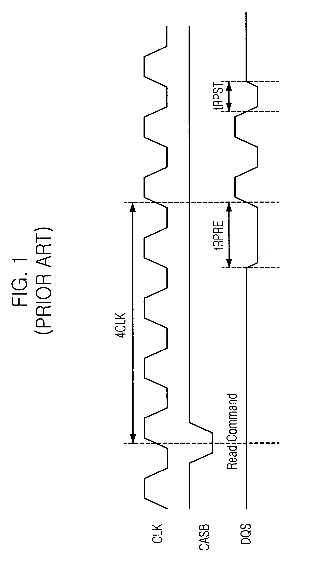
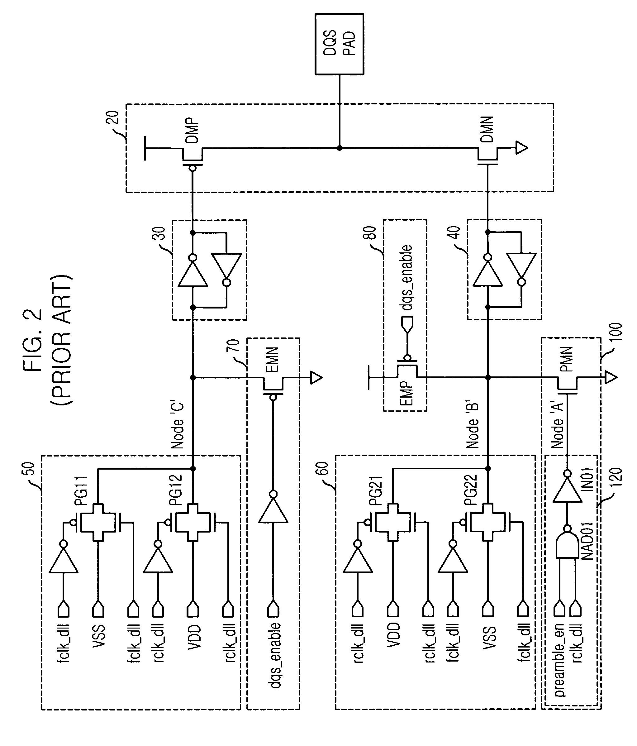
[0025]A data strobe signal generating circuit in accordance with an embodiment of the present invention uses a preamble signal preamble_en so as to guarantee a preamble period tRPRE. Since at least one operating clock must be guaranteed as the preamble period tRPRE, the preamble signal preamble_en must be enabled earlier than a completion timing of a CAS latency CL by “one clock+α”. Since a configuration to generate the preamble signal preamble_en is disclosed in Korean Patent Application NO. 10-2002-0017266, filed by the present applicant, a detailed description thereof will be omitted.

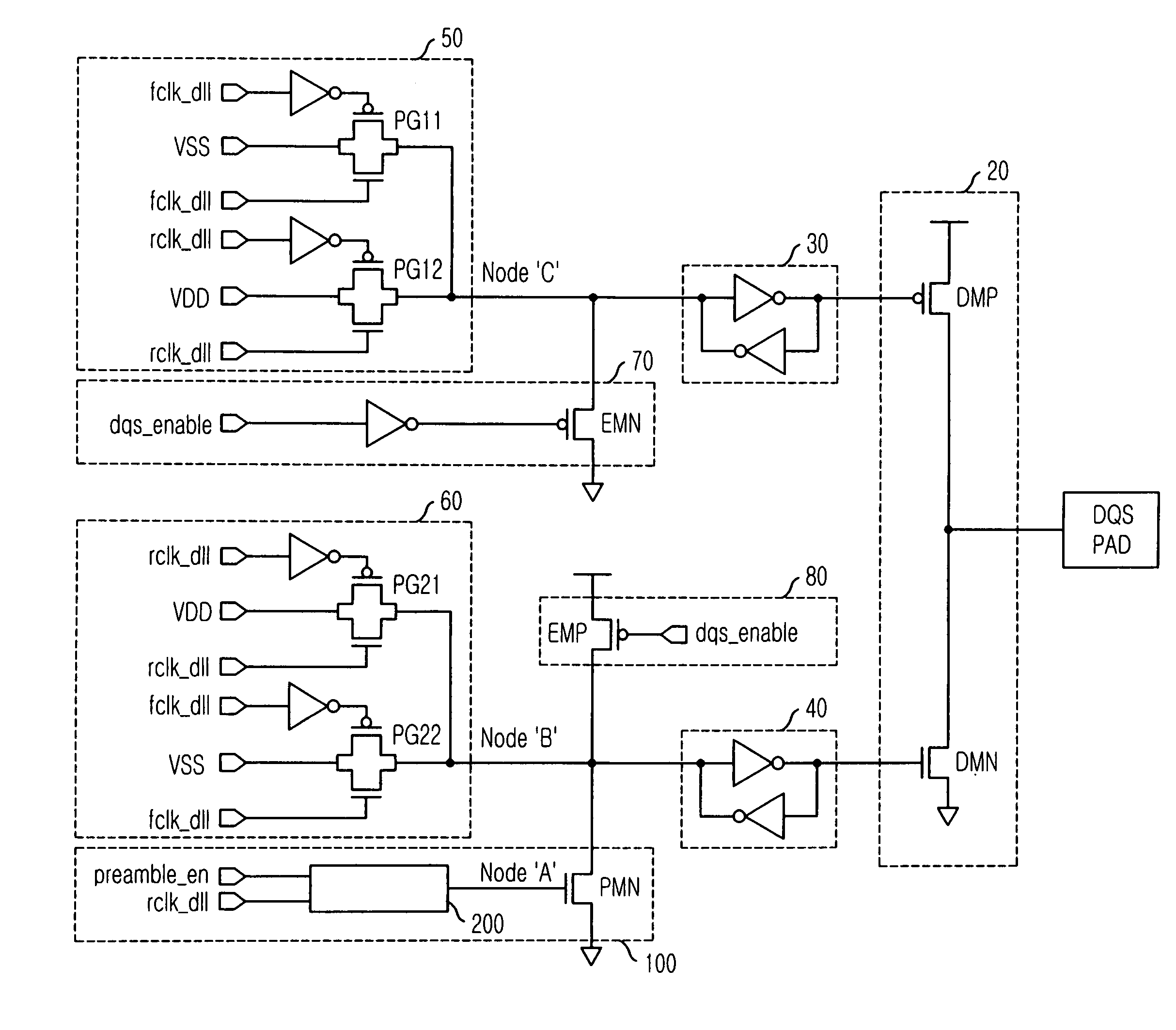
[0026]FIG. 4 is a circuit diagram of a data strobe signal generating circuit according to a preferred embodiment of the present invention.

[0027]Referring to FIG. 4, the data strobe signal generating circuit in...


PUM


Abstract

Provided is a data strobe signal generating circuit capable of guaranteeing a preamble time (tRPRE). The data strobe signal generating circuit includes: a strobe output driver for outputting a data strobe signal to an outside of a semiconductor device so as to indicate synchronization between an external device and data input / output; and a preamble part for maintaining an output of the strobe output driver to a predetermined logic level during a predetermined delay time from an enabling timing of the preamble signal. Accordingly, it is possible to guarantee the stable operation of the semiconductor memory even when PVT (processor, operating voltage, operating temperature) changes.

Description

FIELD OF INVENTION[0001]The present invention relates to a data strobe signal (DQS) generating circuit in which a data strobe signal is generated in synchronization with an external device in a read / write operation of a semiconductor memory device; and, more particularly, to a data strobe signal generating circuit that is capable of guaranteeing a read DQS preamble time (tRPRE), which is a margin where the data strobe signal generating circuit is driven earlier than an output timing of data stored in a memory cell in a read operation of a semiconductor memory device.DESCRIPTION OF PRIOR ART[0002]FIG. 1 is a waveform of a clock CLK, a CAS pulse CASB and a data strobe signal DQS in a read operation of a conventional semiconductor memory device when a CAS latency is four clocks and a burst length is four. The environment condition required in the waveform of FIG. 1 is that four data must be outputted after four clocks from an input of a read command and a data strobe signal DQS must be...

Claims


Application Information

Patent Timeline
Patent Type & Authority Patents(United States)
IPC IPC(8): H03K3/017H03B1/00
CPCG11C7/1051G11C7/1057G11C7/1066G11C7/1093G11C7/22G11C7/222G11C7/10G11C8/00G11C8/18
Inventor PARK, KI-CHON
Owner SK HYNIX INC
Why Eureka
Try Eureka