
Method of fabricating MIM capacitor

a capacitor and mim technology, applied in capacitors, semiconductor devices, semiconductor/solid-state device details, etc., can solve the problem that the capacitor fabricating method cannot increase the size of the capacitor to provide sufficient capacitance, and achieve the effect of increasing the effective area of the capacitor and increasing the capacitan

Inactive Publication Date: 2007-06-26
DONGBU ELECTRONICS CO LTD
View PDF10 Cites 7 Cited by
  • Summary
  • Abstract
  • Description
  • Claims
  • Application Information

AI Technical Summary

Benefits of technology

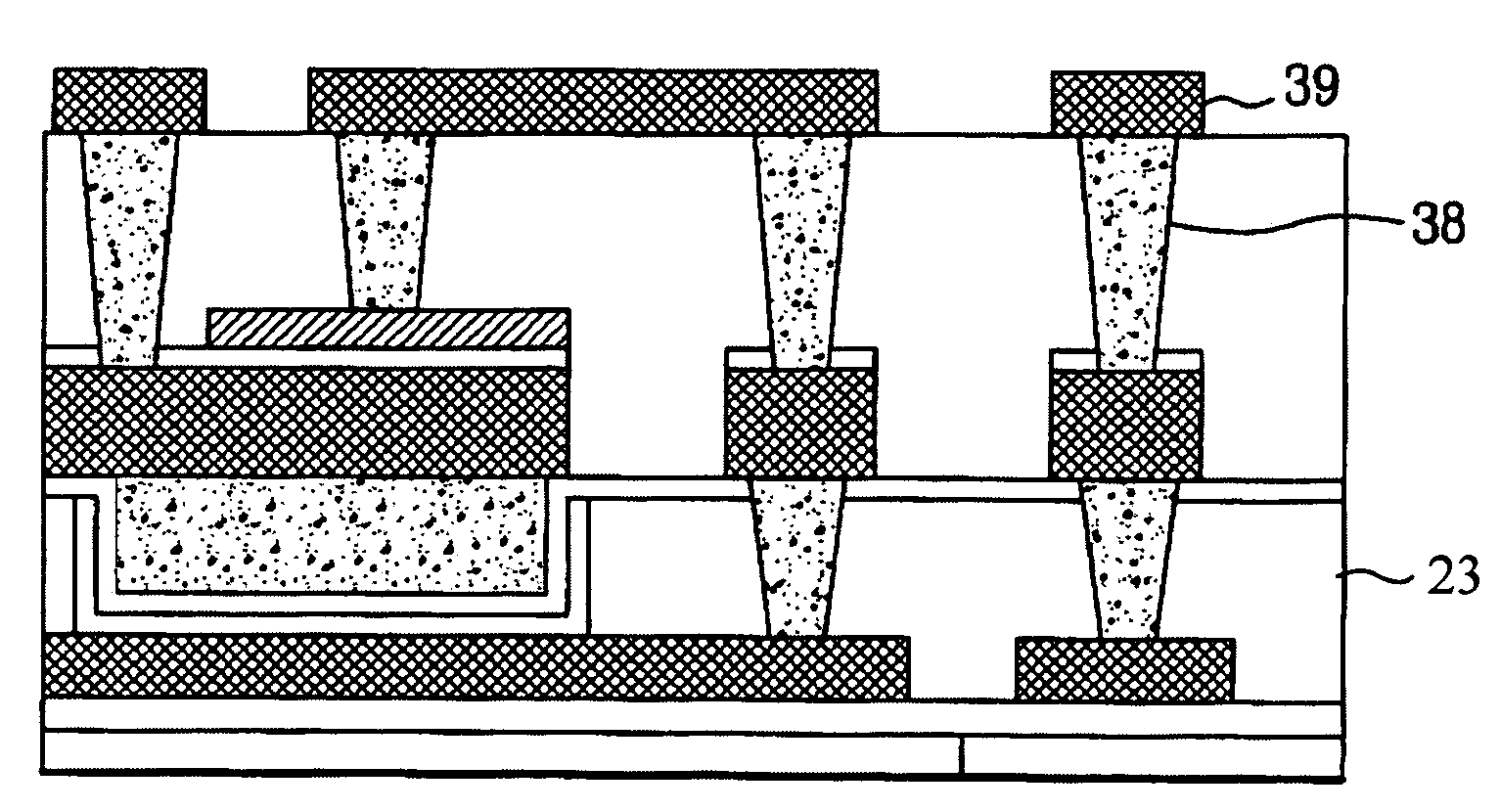
[0020]An object of the present invention is to provide a method of fabricating an MIM capacitor, by which higher capacitance can be secured per unit volume and / or area by forming a dual-stack type capacitor to increase an effective area of the capacitor.

Problems solved by technology

However, the related art capacitor fabricating method cannot increase the size of the capacitor to provide sufficient capacitance for certain applications without undue area consumption.

Method used


Image

  • Method of fabricating MIM capacitor
  • Method of fabricating MIM capacitor
  • Method of fabricating MIM capacitor

Examples


Embodiment Construction

[0027]Reference will now be made in detail to the preferred embodiments of the present invention, examples of which are illustrated in the accompanying drawings. Wherever possible, the same reference numbers will be used throughout the drawings to refer to the same or like parts.

[0028]FIGS. 2A to 2I are cross-sectional diagrams for explaining a method of fabricating a capacitor according to the present invention.

[0029]FIG. 2A shows steps of forming a first insulating layer and a first metal layer in turn on a substrate provided with prescribed devices formed therein, patterning the first metal layer, forming a second insulating layer, and then planarizing the second insulating layer.

[0030]Referring to FIG. 2A, a first insulating layer 21 for insulation from devices below is stacked on a semiconductor substrate on which a conventional FEOL process for semiconductor devices (i.e., transistor formation) has been performed in a general manner. The first insulating layer 21 is then plana...


PUM

PropertyMeasurementUnit
thickaaaaaaaaaa
conductiveaaaaaaaaaa
insulatingaaaaaaaaaa

Abstract

A method of fabricating an MIM capacitor is provided, by which higher capacitance can be secured per unit volume or area by forming a dual-stack type capacitor to increase an effective area of the capacitor. The method includes patterning a first metal layer, forming a planarized second insulating layer having a trench exposing a portion of the patterned first metal layer, forming a second metal layer within the trench, forming a first dielectric layer on the second metal layer, forming first via holes exposing the patterned first metal layer, forming first plugs filling the trench and first via holes, forming a third metal layer thereover, forming a second dielectric layer on the third metal layer, forming a patterned fourth metal layer on the second dielectric layer, patterning the second dielectric layer and the third metal layer, forming a planarized third insulating layer having second via holes therein, and forming a patterned fifth metal layer on the third insulating layer.

Description

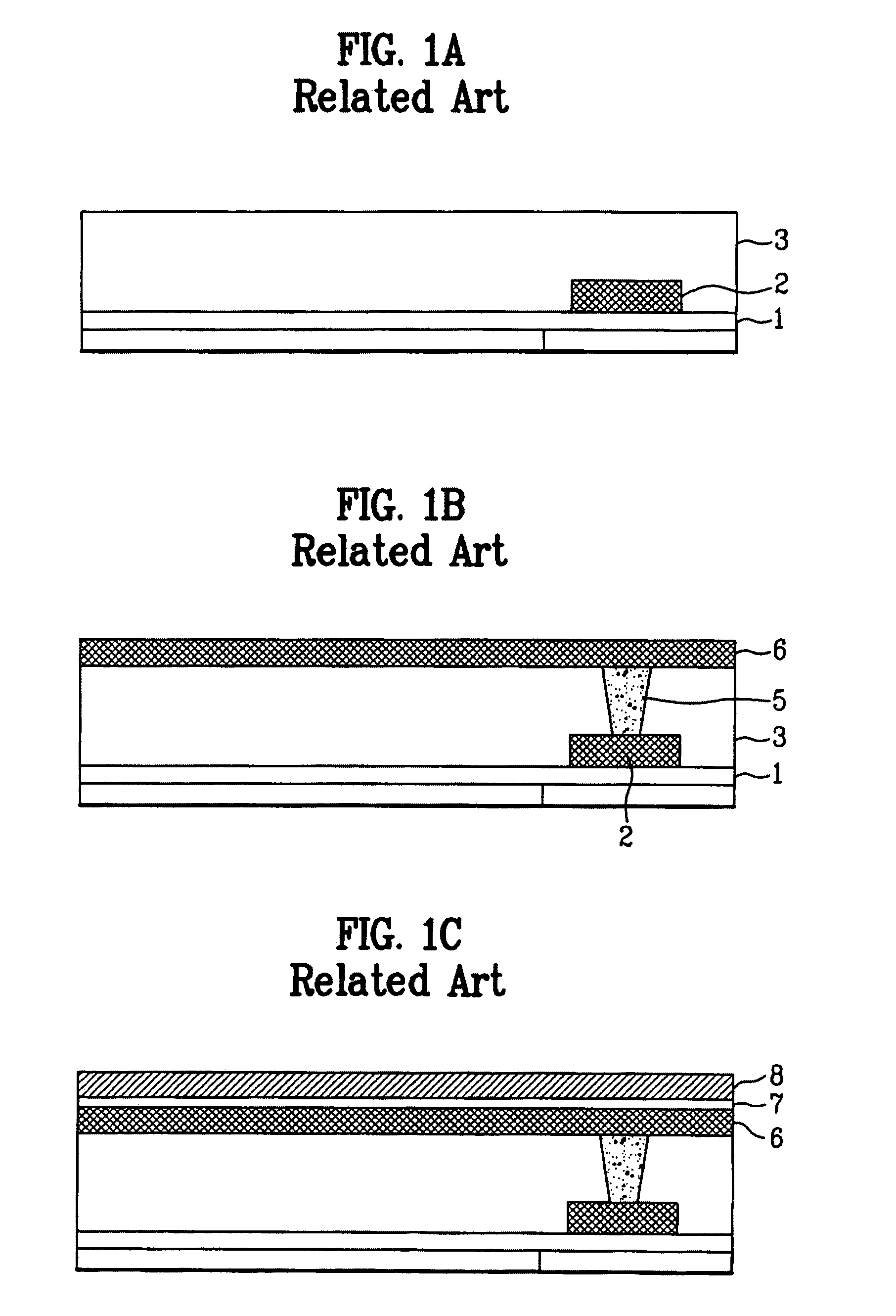
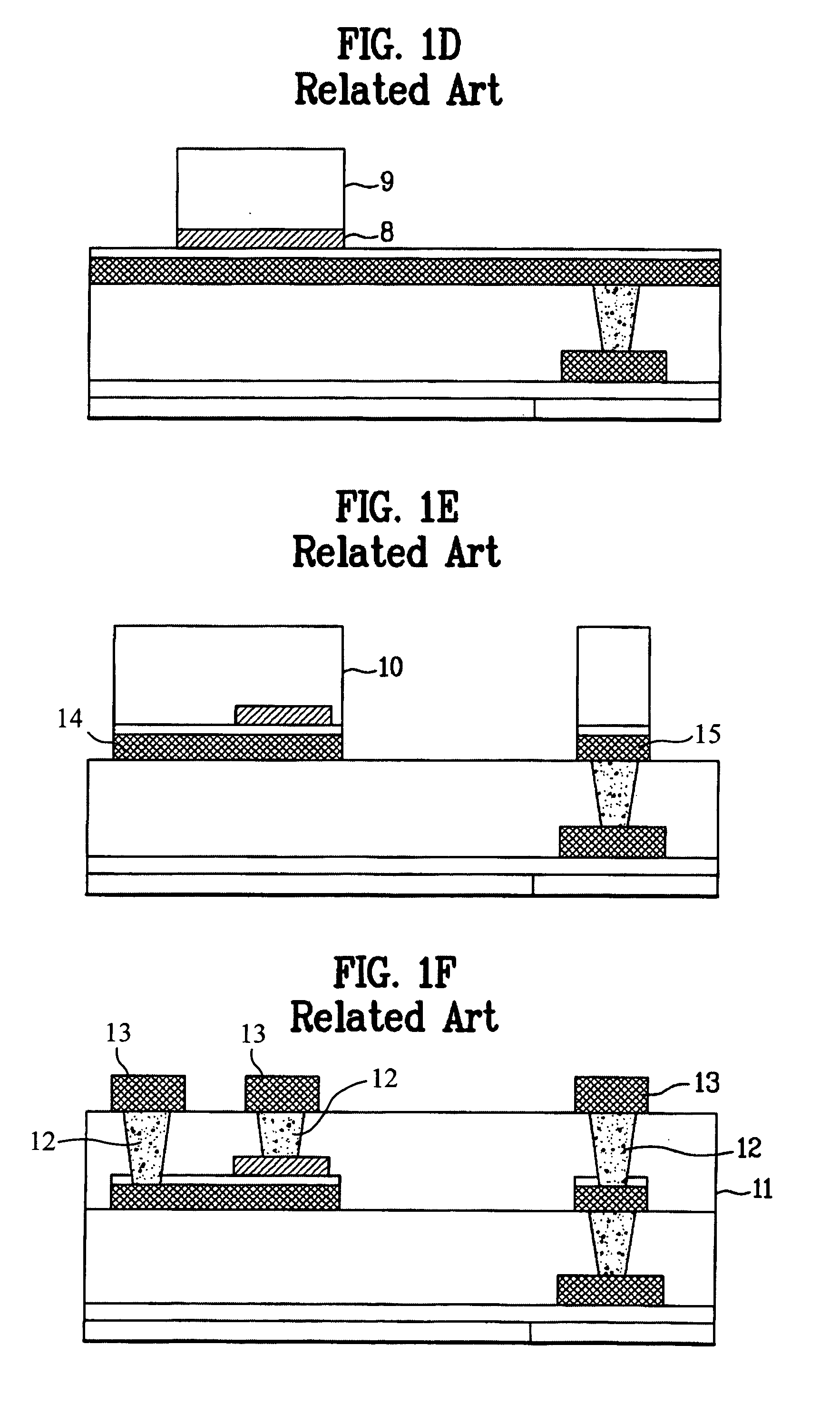
[0001]This application claims the benefit of the Korean Application No. P2003-101605 filed on Dec. 31, 2003, which is hereby incorporated by reference.BACKGROUND OF THE INVENTION[0002]1. Field of the Invention[0003]The present invention relates to a method of fabricating a semiconductor device, and more particularly, to a method of fabricating an MIM capacitor, by which a dual-stack structure can be provided using a general logic forming process.[0004]2. Discussion of the Related Art[0005]FIGS. 1A to 1F are cross-sectional diagrams for explaining a capacitor fabricating method according to a related art.[0006]FIG. 1A shows a step of forming a first conductive layer and an insulating layer on a semiconductor substrate.[0007]Referring to FIG. 1A, a first insulating film 1 for insulation from devices below is stacked on a semiconductor substrate on which the FEOL process of a semiconductor device (i.e., transistor formation) has been performed in a general manner. The first insulating ...

Claims


Application Information

Patent Timeline
Patent Type & Authority Patents(United States)
IPC IPC(8): H01L21/20H01L27/108H01L21/02H01L23/522
CPCH01L23/5223H01L28/40H01L2924/0002H01L2924/00H10B12/00
Inventor KIM, YUNG PIL
Owner DONGBU ELECTRONICS CO LTD
Learn More