Planarizing device and a planarization method for semiconductor substrates

Inactive Publication Date: 2007-07-03
OKAMOTO MACHINE TOOL WORKS LTD
View PDF16 Cites 56 Cited by
  • Summary
  • Abstract
  • Description
  • Claims
  • Application Information

AI Technical Summary

Benefits of technology

[0035]Process 1 typically includes seizing a substrate that is stored in a storage cassette of the substrate storage stage with suction/gripping pads of the multi-joint tr

Problems solved by technology

The grinding process described in Japanese Unexamined Patent Publication No. 2005-98773 is performed on the substrate holder on the index rotary table, and the polishing process is performed on the other substrate holder table, but its throughput is 12-13 sheets per hour with a 300 mm diameter substrate a

Method used


Image

  • Planarizing device and a planarization method for semiconductor substrates
  • Planarizing device and a planarization method for semiconductor substrates
  • Planarizing device and a planarization method for semiconductor substrates

Examples


Embodiment Construction

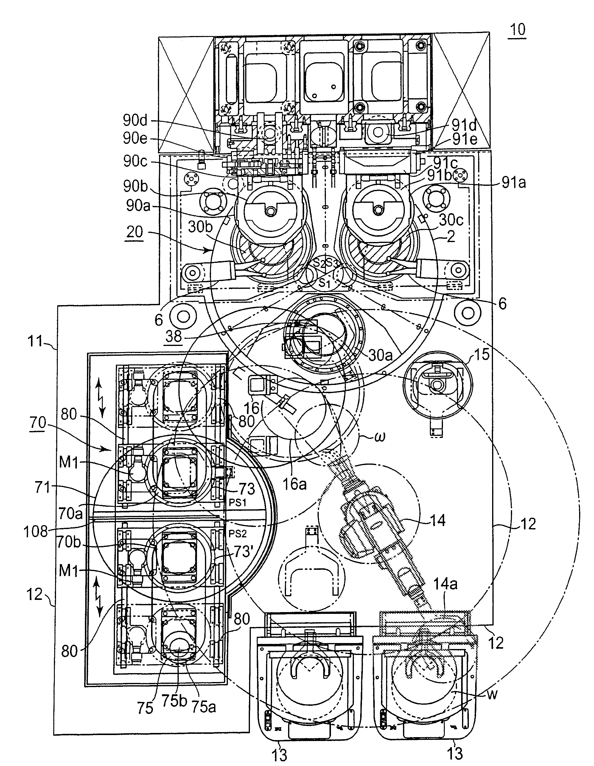
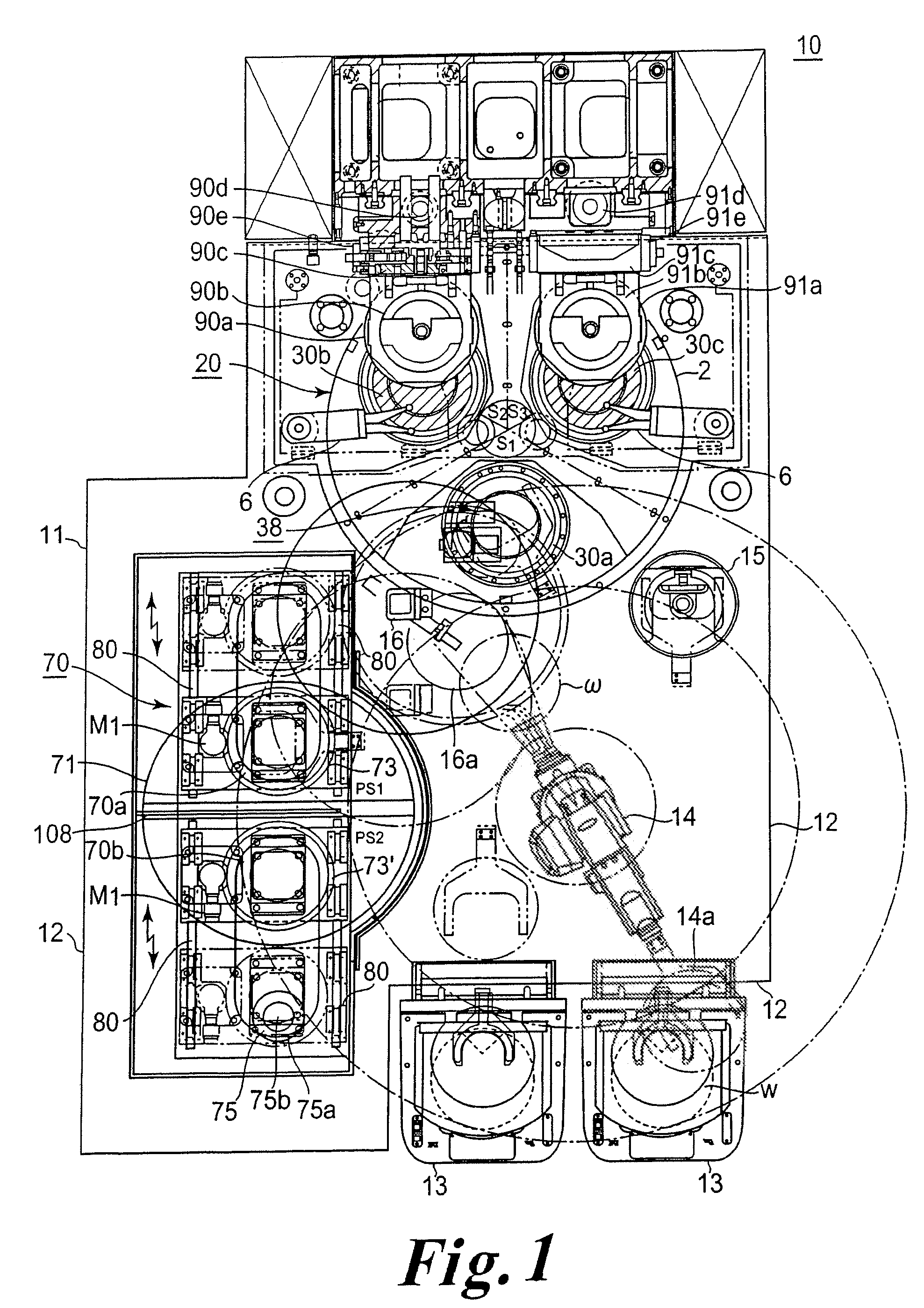
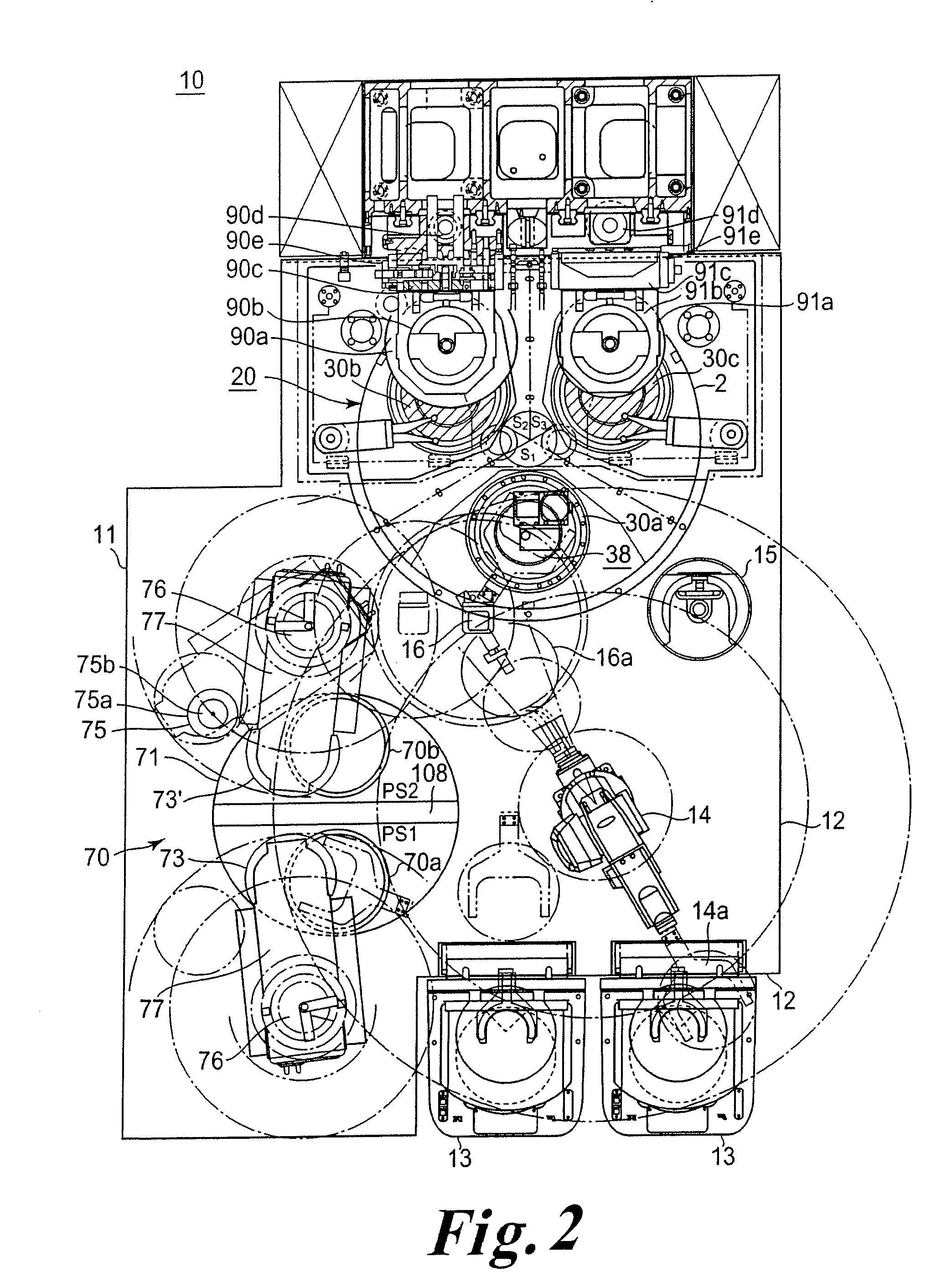
[0055]Referring now to the drawings, wherein like reference numerals designate identical or corresponding parts throughout the several views.

[0056]In the back area of two non-limiting embodiments of the semiconductor substrate-planarizing device 10 shown in FIG. 1 and FIG. 2, the planarizing device 10 is composed of the substrate storage stage 13 outside of the room divider 12, and inside of the room divider 12 on the base 11, the multi-joint transfer robot 14, the temporary alignment platform 15, the grinding process stage 20, the movable transfer pad 16, the polishing process stage 70, and the cleaning device 38 inside the room. It is typically possible to store 25 sheets of the substrates inside of the storage cassette of the substrate storage stage 13.

[0057]In each stage, toward the rear from the front of the planarizing device 10, the substrate storage stage 13 is typically set on the right side of the outside of the room, and the multi-joint transfer robot 14 equipped with the...


PUM

PropertyMeasurementUnit
Angleaaaaaaaaaa
Angleaaaaaaaaaa
Angleaaaaaaaaaa

Abstract

A substrate-planarizing device and method of using the device comprising a substrate storage stage outside a room, and on a base inside the room, a multi-joint transfer robot, a temporary alignment platform, a movable transfer pad, a grinding process stage in which substrate holders that compose three stages of a substrate loading/unloading stage, a rough grinding stage, a finish grinding stage are arranged in a concentric pattern on the first index rotary table, and a polishing process stage that has a substrate holder table composing a substrate loading/unloading/finish polishing stage as well as a substrate holder table composing a rough polishing stage arranged in a concentric pattern on the second index rotary table.

Description

CROSS REFERENCE TO RELATED APPLICATION[0001]The present application claims priority to Japanese Patent Application No. JP 2006-090114, filed Mar. 29, 2006, the entire contents of which are incorporated herein by reference.BACKGROUND OF THE INVENTION[0002]1. Field of the Invention[0003]The present invention relates to a planarizing device and method, which is used for thinning and planarizing substrates by grinding and polishing the back surface of the semiconductor substrates in a preprocessing process of IC substrates.[0004]2. Description of the Related Art[0005]In a background planarizing device, semiconductor substrates are ground / polished for thinning and mirror finishing. Multiple substrate holder tables can retain substrates by vacuum suction are arranged in a lower side, and a rotating spindle comprising a rough grinding wheel, a rotating spindle comprising a finish grinding wheel, and a rotating spindle comprising polishing equipments is arranged on top of each of multiple s...

Claims


Application Information

Patent Timeline
IPC IPC(8): B24B1/00B24B7/00B24B37/04H01L21/304
CPCB24B7/228B24B37/04B24B41/005B24B51/00H01L21/304
Inventor KASHIWA, MORIYUKIOKONOGI, HIROTAKAKOBAYASHI, KAZUO
Owner OKAMOTO MACHINE TOOL WORKS LTD
Why Eureka
Try Eureka