
Memory device, memory managing method and program

a memory management and memory device technology, applied in the field of memory devices, memory managing methods and programs, can solve the problems of long time needed to rewrite or erase data, data reading took time, and the type had a difficulty in sufficiently preventing the occurrence of defective blocks, etc., to achieve data renewal and erasure faster

Inactive Publication Date: 2007-07-10
TOKYO ELECTRON DEVICE
View PDF10 Cites 28 Cited by
  • Summary
  • Abstract
  • Description
  • Claims
  • Application Information

AI Technical Summary

Benefits of technology

"The invention provides a memory device and method that can quickly and efficiently renew and erasure data. The device includes a memory with multiple memory blocks, each containing one or more physical pages with logical pages. When new data is written, the device assigns a new empty logical page for storing the data and indicates that the previous data is invalid. This prevents unnecessary flash erase on memory blocks and slows down the degrading of the memory device. The method also allows for the allocation of physical addresses to logical pages and the efficient management of data renewal and erasure. Overall, the invention provides a faster and more efficient way to manage data in a memory device."

Problems solved by technology

Of flash memories, particularly, a NAND type has a difficulty in sufficiently preventing the occurrence of defective blocks which cannot carry out the proper data storage at the manufacturing stage.
Therefore, data reading took time, which would eventually make the time needed to rewrite or erase data very long as a whole.
While a NAND type flash memory can achieve a large-capacity structure at a low cost, it would be too degraded to perform proper data reading and writing by repetitive flash erase.
Therefore, the execution of the aforementioned operation rewrites a small amount of data, which results in inefficient frequent flash erase.

Method used


Image

  • Memory device, memory managing method and program
  • Memory device, memory managing method and program
  • Memory device, memory managing method and program

Examples


Embodiment Construction

[0048]One embodiment of the invention will be described below, taking a memory system equipped with a flash memory as an example, with reference to the accompanying drawings.

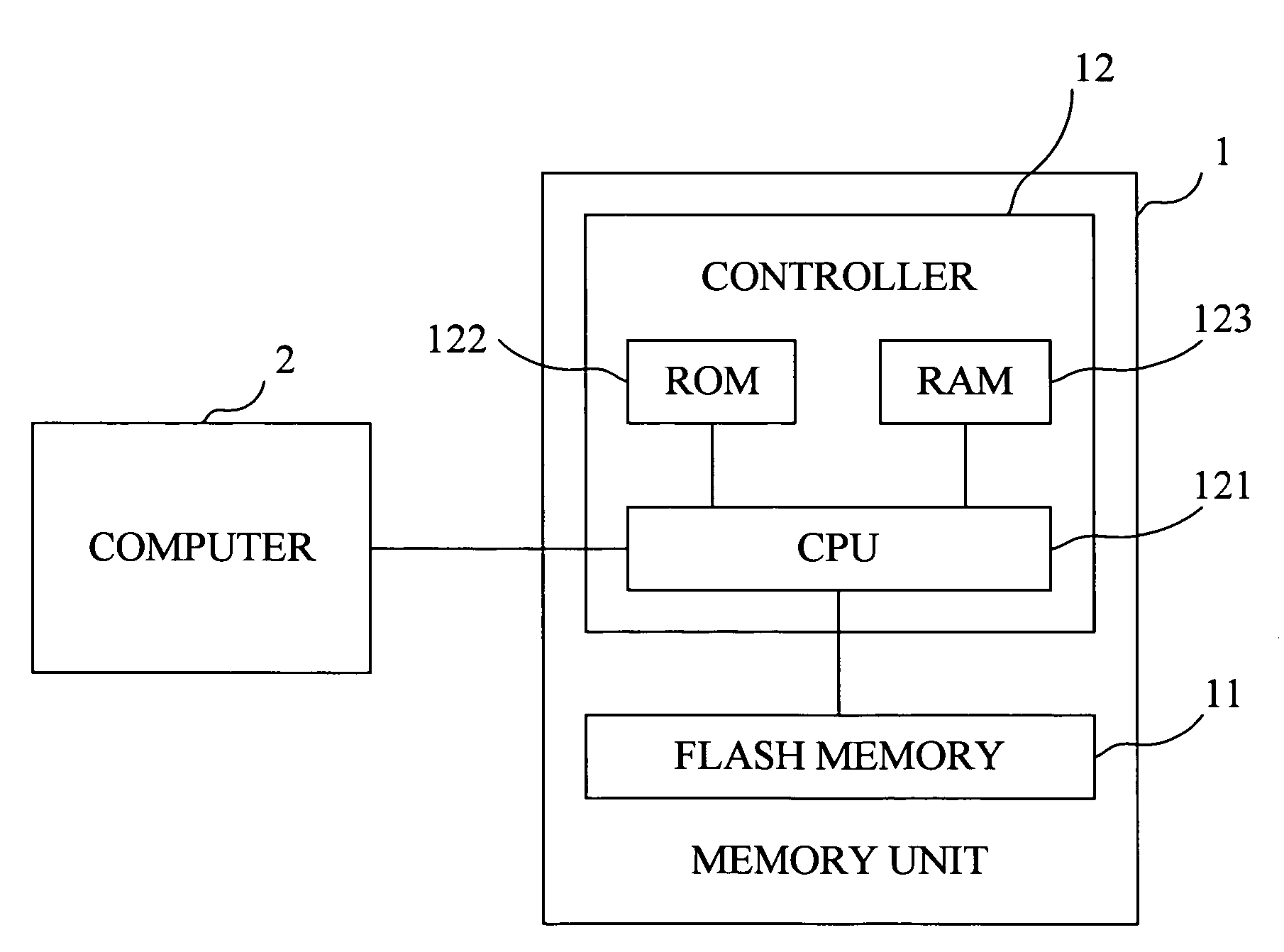
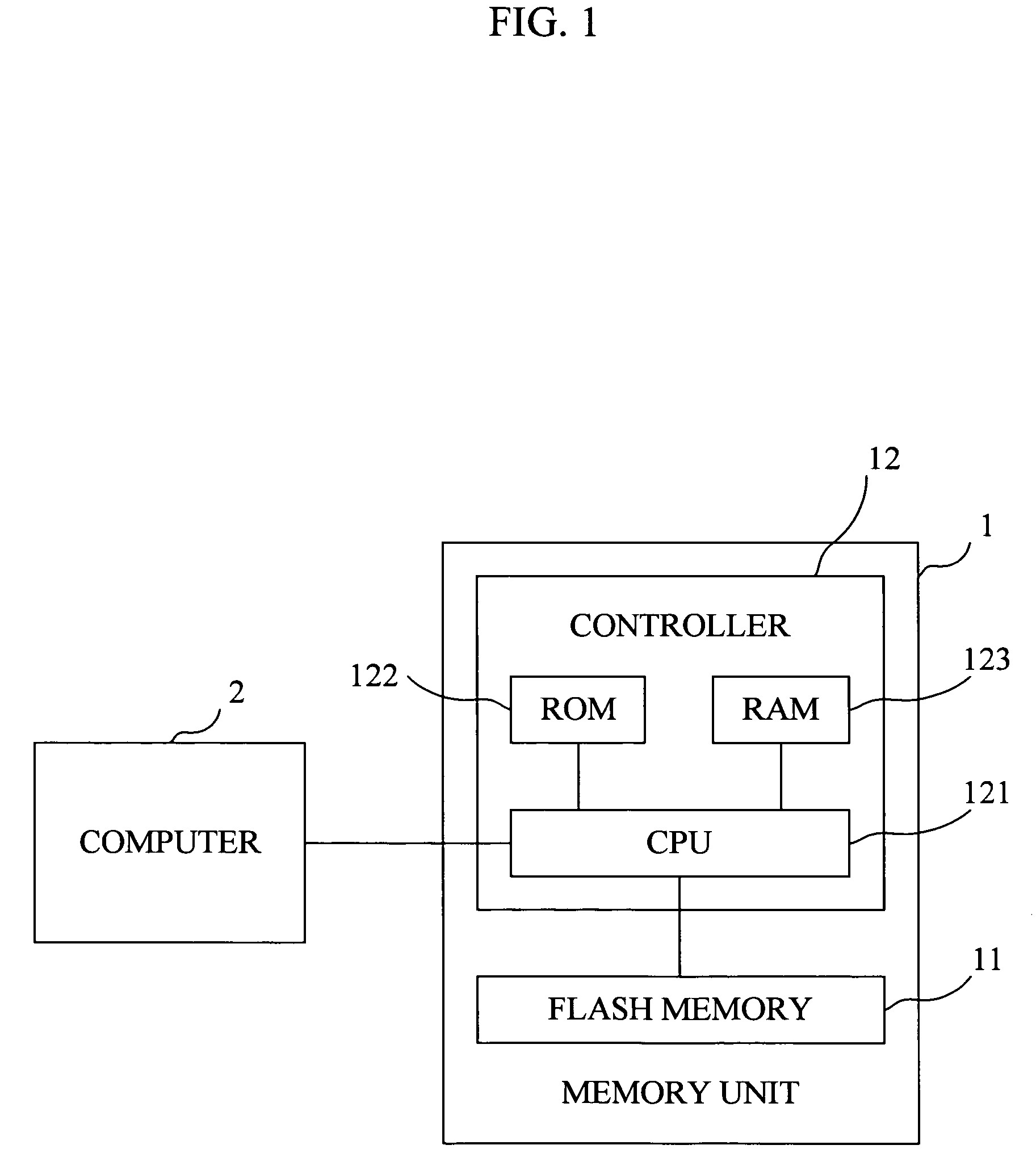
[0049]FIG. 1 is a block diagram illustrating the physical structure of the memory system according to the embodiment of the invention.

[0050]As illustrated, the memory system comprises a memory unit 1 and a computer 2. The memory unit 1 is attached in a detachable manner to the computer 2 via a slot provided in the computer 2.

[0051]The slot of the computer 2 comprises, for example, a PCMCIA slot for relaying a PCMCIA bus.

[0052]The memory unit 1 comprises a flash memory 11 and a controller 12.

[0053]The flash memory 11 is comprised of a memory device, such as EEPROM (Electrically Erasable / Programmable Read Only Memory).

[0054]In response to an access made by the controller 12, the flash memory 11 stores data supplied from the computer 2, supplies stored data to the computer 2 and erases stored data.

[0055]The memory ...


PUM


Abstract

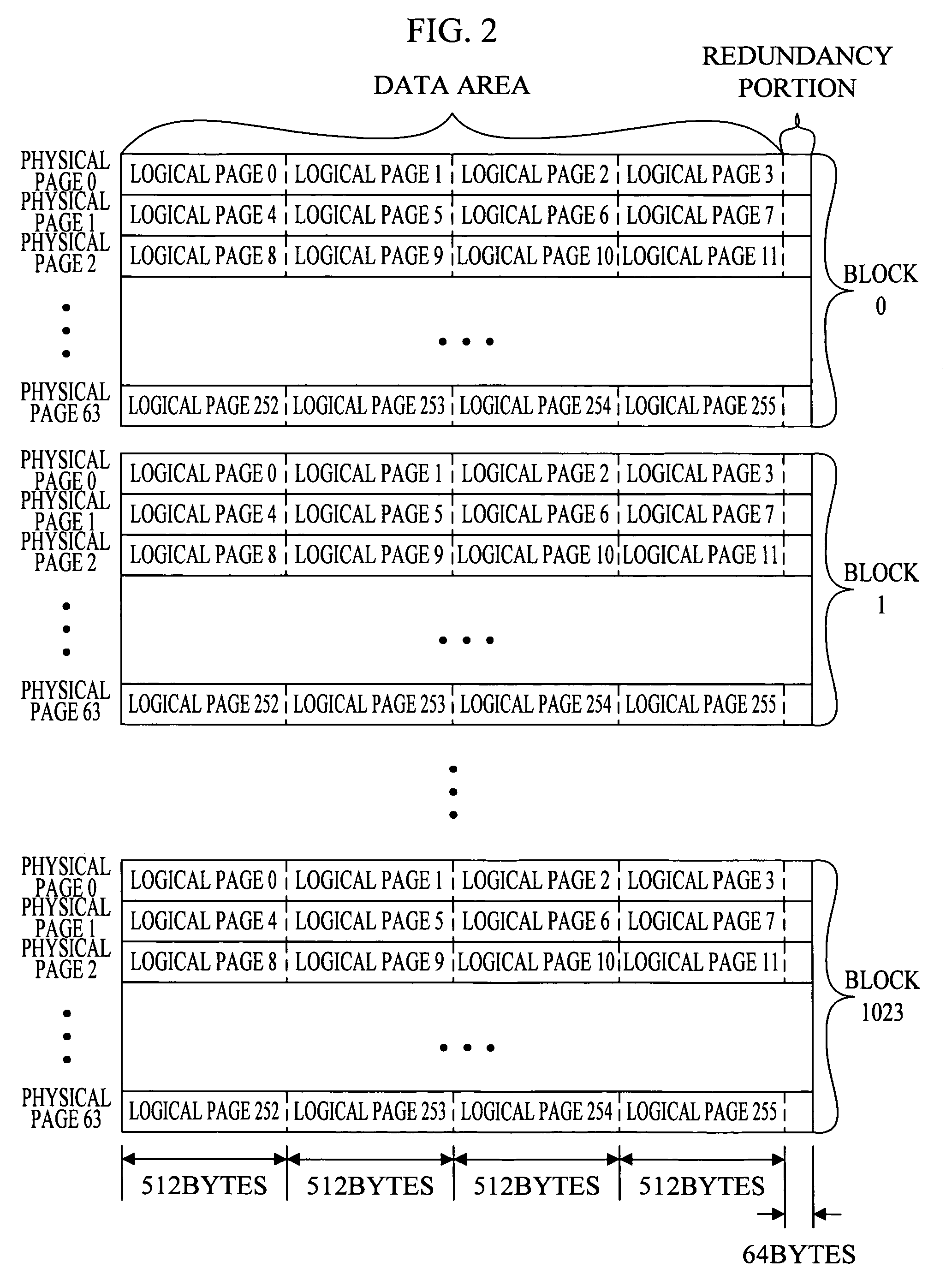
A memory device, performs fast data renewal and erasure, and is not easily degraded. In the memory area of a flash memory, each block is divided into physical pages and each physical pages is divided into logical pages. A redundancy portion is provided for each physical page. When supplied with to-be-written data and the logical address of a write destination, a CPU writes this data in an empty logical page and allocates the supplied logical address to this logical page. An old data flag in the redundancy portion in that physical page which includes a logical page having old data stored therein is changed in such a way as to indicate that data in this logical page is invalid. New data writing is done in that logical page to which a logical address is not allocated. At the time of flash-erasing a block, data which is stored in that logical page which is indicated by the old data flag is not transferred.

Description

TECHNICAL FIELD[0001]The present invention relates to a memory device, a memory managing method and a program, and, more particularly, to a block erasure type memory device, and a memory managing method and a program which manage a block erasure type memory device.BACKGROUND ART[0002]In addition to a hard disk unit and a floppy (registered trademark) disk, an EEPROM (Electrically Erasable / Programmable Read Only Memory) flash memory is used as a recording medium which is accessible (data readable and erasable) by a computer or the like. In case where a flash memory is used to store files under the control of a disk operating system, such as MS-DOS (registered trademark) or Windows (registered trademark), each of which is a product of Microsoft Corporation, the control becomes easy if a scheme using data read / write units (e.g., 512 bytes), which has conventionally been used at the time of using a hard disk unit, is employed.[0003]The unit of the memory capacity of a flash memory in ca...

Claims


Application Information

Patent Timeline
Patent Type & Authority Patents(United States)
IPC IPC(8): G11C8/00G06F3/06G06F12/02
CPCG06F3/061G06F3/0616G06F3/064G06F3/0679G06F12/0246
Inventor HIRAKA, SEIJI
Owner TOKYO ELECTRON DEVICE
Learn More