Semiconductor device and method for manufacturing the same

a semiconductor and display technology, applied in the field of semiconductor devices, can solve the problems of increased manufacturing steps and inability to function well of back gate electrodes, and achieve the effects of fewer steps, improved semiconductor devices, and easy normal o

Active Publication Date: 2014-03-25
SEMICON ENERGY LAB CO LTD
View PDF144 Cites 22 Cited by
  • Summary
  • Abstract
  • Description
  • Claims
  • Application Information

AI Technical Summary

Benefits of technology

[0010]It is an object of one embodiment of the present invention to manufacture a semiconductor device including a bottom-gate transistor with a back gate electrode in fewer steps. Alternatively, it is an object of one embodiment of the present invention to provide a semiconductor device including a bottom-gate transistor with a back gate electrode that can be manufactured in fewer steps. Alternatively, it is an object of one embodiment of the present invention to provide a semiconductor device where a strong electric field can be applied to a semiconductor layer by a back gate electrode. Alternatively, it is an object of one embodiment of the present invention to provide a semiconductor device where the threshold voltage is controlled. Alternatively, it is an object of one embodiment of the present invention to provide a semiconductor device which is easily normally off. Alternatively, it is an object of one embodiment of the present invention to provide a semiconductor device including a transistor whose on-state current is high. Alternatively, it is an object of one embodiment of the present invention to provide a semiconductor device including a transistor capable of inhibiting the incidence of light on a channel or the like. Alternatively, it is an object of one embodiment of the present invention to provide a semiconductor device including a transistor which is not easily degraded. Alternatively, it is an object of one embodiment of the present invention to provide a semiconductor device where the thickness of an insulating layer provided over a channel of a transistor is varied using a half-tone mask or a gray-tone mask. Alternatively, it is an object of one embodiment of the present invention to provide a better semiconductor device while inhibiting an increase in the number of steps. Alternatively, it is an object of one embodiment of the present invention to provide a semiconductor device where an increase in cost is inhibited by inhibiting an increase in the number of steps. Alternatively, it is an object of one embodiment of the present invention to provide a display device capable of displaying an image accurately by using a transistor whose off-state current is low. Alternatively, it is an object of one embodiment of the present invention to provide a display device having a high aperture ratio. Alternatively, it is an object of one embodiment of the present invention to provide a semiconductor device in which noise to a pixel electrode is low. Alternatively, it is an object of one embodiment of the present invention to provide a semiconductor device in which an insulating layer is thicker in a portion below a pixel electrode than in a portion below a back gate electrode.
[0018]According to one embodiment of the present invention, it is possible to manufacture a semiconductor device including a bottom-gate transistor with a back gate electrode in fewer steps. Alternatively, it is possible to provide a semiconductor device including a bottom-gate transistor with a back gate electrode that can be manufactured in fewer steps. Alternatively, it is possible to provide a semiconductor device where a strong electric field can be applied to a semiconductor layer by a back gate electrode. Alternatively, it is possible to provide a semiconductor device where the threshold voltage is controlled. Alternatively, it is possible to provide a semiconductor device which is easily normally off. Alternatively, it is possible to provide a semiconductor device including a transistor whose on-state current is high. Alternatively, it is possible to provide a semiconductor device where the thickness of an insulating layer provided over a channel of a transistor is varied using a half-tone mask, a gray-tone mask, a phase shift mask, or a multi-tone mask. Alternatively, it is possible to provide a better semiconductor device while inhibiting an increase in the number of steps. Alternatively, it is possible to provide a semiconductor device where an increase in cost is inhibited by inhibiting an increase in the number of steps. Alternatively, it is possible to provide a display device capable of displaying an image accurately by using a transistor whose off-state current is low. Alternatively, it is possible to provide a display device having a high aperture ratio. Alternatively, it is possible to provide a display device in which noise to a pixel electrode is low. Alternatively, it is possible to provide a display device in which an insulating layer is made thicker in a portion below a pixel electrode than in a portion below a back gate electrode.

Problems solved by technology

Thus, the display device disclosed in Patent Document 1 has a problem in that the number of manufacturing steps is increased as compared to a display device including a transistor which does not have a back gate electrode.
Since the planarization insulating layer is generally thick, there is a problem in that the back gate electrode cannot function well.

Method used


Image

  • Semiconductor device and method for manufacturing the same
  • Semiconductor device and method for manufacturing the same
  • Semiconductor device and method for manufacturing the same

Examples


embodiment 1

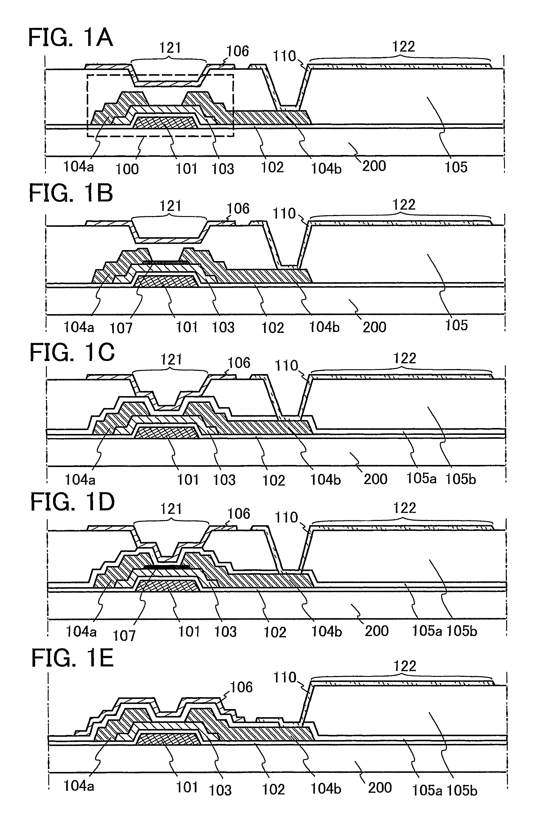
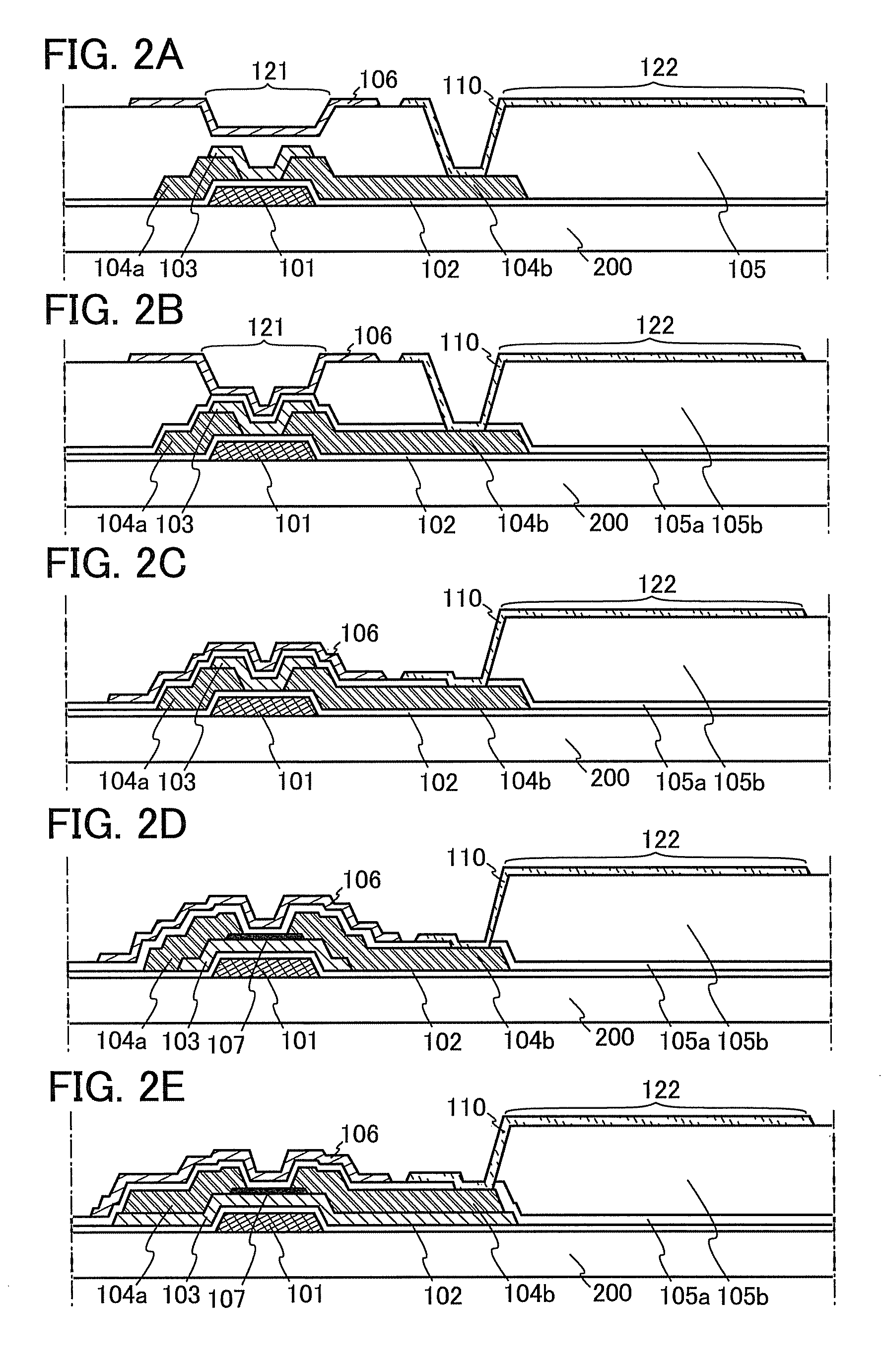
[0101]In this embodiment, one aspect of a semiconductor device or the like (e.g., a display device or a light-emitting device) in the present invention is described with reference to drawings.

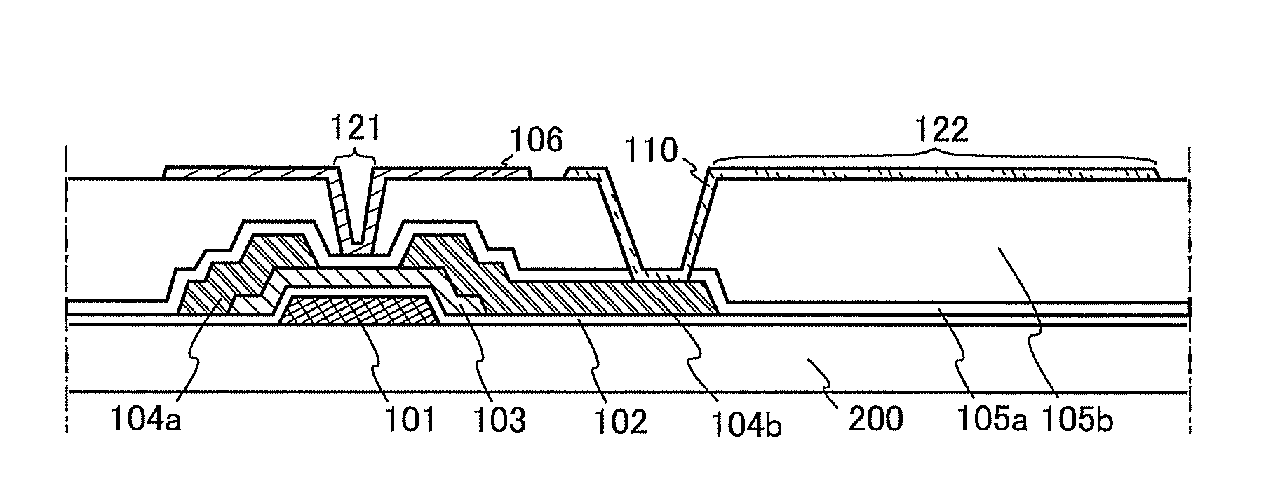
[0102]FIG. 1A is a cross-sectional view of a semiconductor device in one embodiment of the present invention. The semiconductor device includes a transistor 100 and an electrode 110 over an insulating surface (or an insulating substrate) 200. The transistor 100 includes an electrode 101, an insulating layer 102 over the electrode 101, a semiconductor layer 103 over the insulating layer 102, an insulating layer 105 over the semiconductor layer 103, and an electrode 106 over the insulating layer 105. The electrode 101 has a region overlapping with the semiconductor layer 103 with the insulating layer 102 provided therebetween. The electrode 106 has a region overlapping with the semiconductor layer 103 with the insulating layer 105 provided therebetween. The electrode 110 is provided over the insu...

embodiment 2

[0128]In this embodiment, one aspect of a semiconductor device or the like (e.g., a display device or a light-emitting device) in the present invention is described with reference to drawings.

[0129]In the structure described in Embodiment 1 with reference to FIG. 1A, FIG. 1B, FIG. 2A, FIG. 3A, FIG. 3B, FIG. 9A, or the like, the insulating layer 105 in the region 122 or part of the region 122 can include a stack of a plurality of layers. The insulating layer 105 in the region 122 or part of the region 122 includes a stack of m (m is a natural number of 2 or more) layers. The insulating layer 105 in the region 121 or part of the region 121 may include a stack of m or less layers or a single layer. The insulating layer 105 may include an organic insulating layer or a stack of an organic insulating layer and an inorganic insulating layer.

[0130]For example, in the structure illustrated in FIG. 1A, FIG. 1B, FIG. 2A, FIG. 3A, FIG. 3B, FIG. 9A, or the like, the insulating layer 105 in the r...

embodiment 3

[0146]In this embodiment, one aspect of a semiconductor device or the like (e.g., a display device or a light-emitting device) in the present invention is described with reference to drawings.

[0147]In the structure described in Embodiment 1 with reference to FIG. 1A, FIG. 1B, FIG. 2A, FIG. 3A, FIG. 3B, FIG. 9A, or the like, the insulating layer 105 is made thin in the vicinity of the channel of the transistor 100. However, the range of the region (the region 121) where the insulating layer 105 is made thin is not limited thereto. The range of the region 121 may be part of the vicinity of the channel. For example, the structure illustrated in FIG. 1A can be changed into a structure illustrated in FIG. 66A. In FIG. 66A, the range of the region 121 is part of the vicinity of the channel (the range of the region 121 in FIG. 66A is smaller than the range of the region 121 in FIG. 1A). The structures illustrated in other than FIG. 1A can be changed similarly. Alternatively, the range of t...


PUM


Abstract

A semiconductor device includes a pixel electrode and a transistor which includes a first gate electrode, a first insulating layer over the first gate electrode, a semiconductor layer over the first insulating layer, a second insulating layer over the semiconductor layer, and a second gate electrode. The pixel electrode and the second gate electrode are provided over the second insulating layer. The first gate electrode has a region overlapping with the semiconductor layer with the first insulating layer provided therebetween. The second gate electrode has a region overlapping with the semiconductor layer with the second insulating layer provided therebetween. A first region is at least part of a region where the second gate electrode overlaps with the semiconductor layer. A second region is at least part of a region where the pixel electrode is provided. The second insulating layer is thinner in the first region than in the second region.

Description

BACKGROUND OF THE INVENTION[0001]1. Field of the Invention[0002]The present invention relates to semiconductor devices, display devices, light-emitting devices, and methods for manufacturing these devices. In particular, the present invention relates to semiconductor devices, display devices, and light-emitting devices each including a transistor, and methods for manufacturing these devices. The present invention relates to electronic devices including the semiconductor devices, the display devices, or the light-emitting devices.[0003]2. Description of the Related Art[0004]It is known that the on-state current of a transistor including gate electrodes above and below with a semiconductor layer provided therebetween can be increased and that the off-state current of the transistor can be decreased by control of the threshold voltage. A transistor with such a structure is referred to as a double-gate transistor or a dual-gate transistor. In the following description, a transistor with...

Claims


Application Information

Patent Timeline
Patent Type & Authority Patents(United States)
IPC IPC(8): H01L33/08
CPCH01L29/78648H01L29/786H01L27/1225H01L29/7869H01L27/1248H01L29/78603G02F1/136227G02F1/1368G02F1/136286G02F1/1345G02F1/133345H01L27/1259H01L27/1262H10K59/123H10K59/1213H01L29/045
Inventor KIMURA, HAJIME
Owner SEMICON ENERGY LAB CO LTD
Why Eureka
Try Eureka