Semiconductor device and measurement device

a technology of semiconductor devices and measurement devices, which is applied in the direction of semiconductor devices, electrical devices, transistors, etc., can solve the problems of reducing the reliability of the transistor, deteriorating the electrical characteristics of the transistor, and reducing the field-effect mobility of the transistor or an increase in off-state current, so as to achieve stable electrical characteristics, small variation in electrical characteristics, and high reliability

Active Publication Date: 2014-07-03
SEMICON ENERGY LAB CO LTD
View PDF3 Cites 62 Cited by
  • Summary
  • Abstract
  • Description
  • Claims
  • Application Information

AI Technical Summary

Benefits of technology

[0028]According to one embodiment of the present invention, an oxide semiconductor in which the density of localized levels is low can be provided. According to one embodiment of the present invention, a semiconductor device having small variation in electrical characteristics can be provided. According to one embodiment of the present invention, a highly reliable semiconductor device which has stable electrical characteristics can be provided. According to one embodiment of the present invention, a semiconductor device which has favorable electrical characteristics can be provided.

Problems solved by technology

An increase in the interface states causes scattering of carriers or capture of carriers, which results in a decrease in field-effect mobility of a transistor or an increase in off-state current.
Accordingly, an increase in interface state density leads to deterioration of the electrical characteristics of the transistor and a reduction in reliability of the transistor.

Method used


Image

  • Semiconductor device and measurement device
  • Semiconductor device and measurement device
  • Semiconductor device and measurement device

Examples


embodiment 1

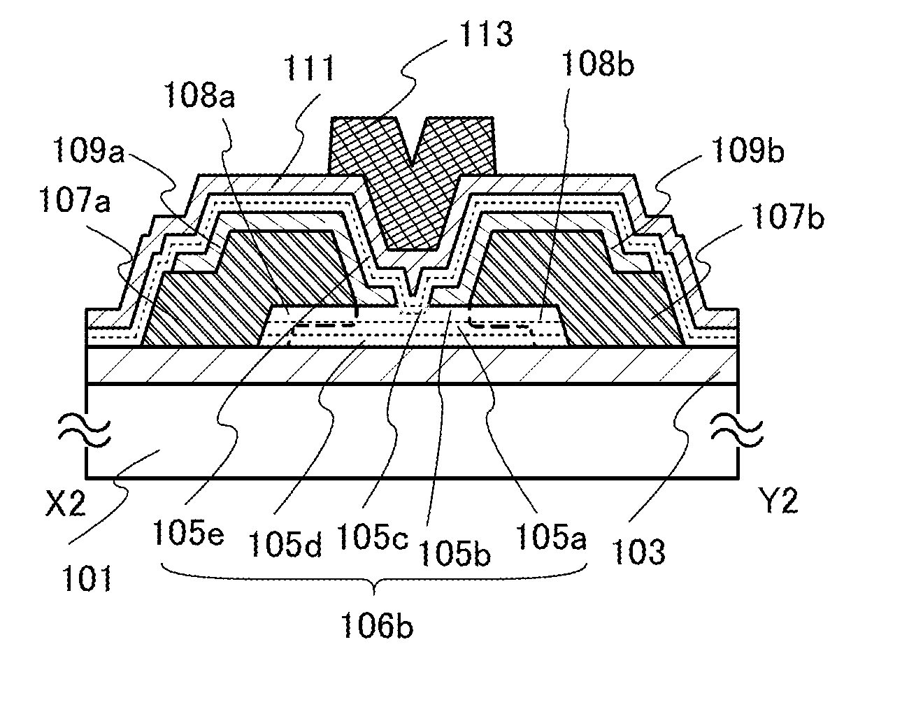
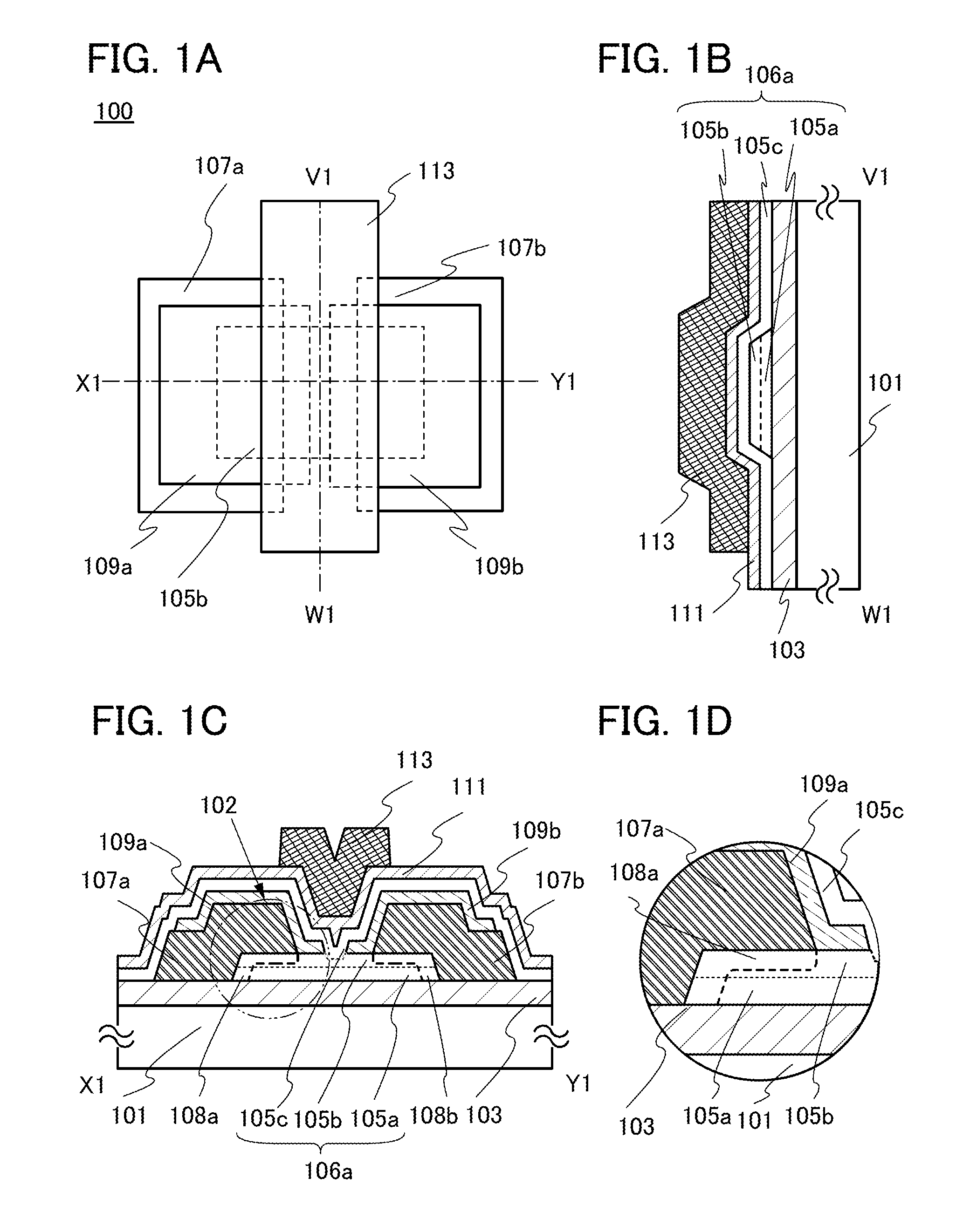
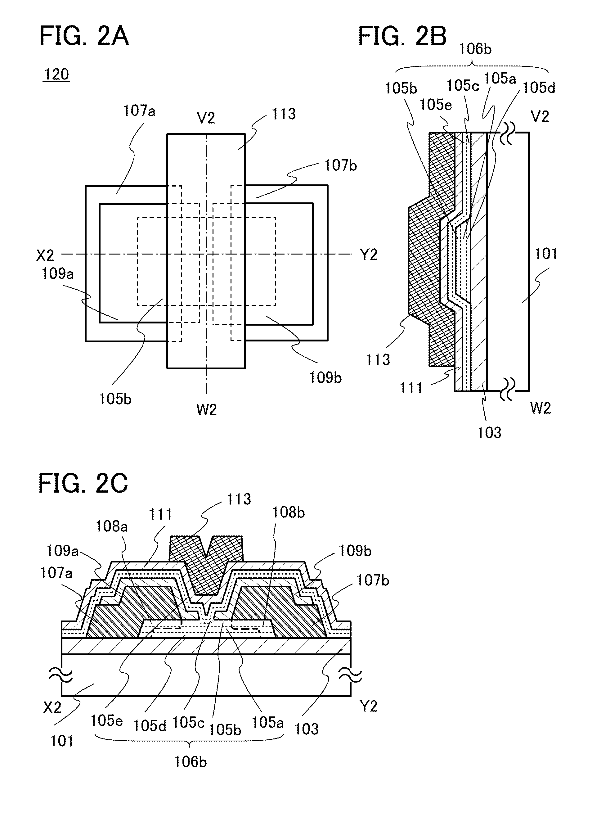
[0095]In this embodiment, a semiconductor device of one embodiment of the present invention is described with reference to FIGS. 1A to 1C, FIGS. 2A and 2B, FIGS. 3A and 3B, FIGS. 4A to 4C, FIGS. 5A and 5B, FIGS. 6A and 6B, and FIGS. 7A to 7D.

[0096]The semiconductor device of one embodiment of the present invention includes a first oxide layer over an insulating surface; an oxide semiconductor layer over the first oxide layer; a first source electrode and a first drain electrode over the oxide semiconductor layer; a second source electrode over the first source electrode; a second drain electrode over the first drain electrode; a second oxide layer over the first source electrode and the first drain electrode; a gate insulating layer which is over the second source electrode, the second drain electrode, and the second oxide layer and is in contact with the top surface of the second oxide layer; and a gate electrode overlapping with the oxide semiconductor layer with the gate insulati...

embodiment 2

[0304]In this embodiment, a manufacturing method of a semiconductor device according to one embodiment of the present invention is described with reference to FIGS. 8A to 8D, FIGS. 9A and 9B, FIGS. 10A and 10B, FIGS. 11A and 11B, FIGS. 12A to 12C, and FIGS. 13A and 13B.

[0305]As an example of a method for manufacturing a semiconductor device of one embodiment of the present invention, an example of a method for manufacturing the transistor 100 is described with reference to FIGS. 8A to 8D.

[Formation of Insulating Layer]

[0306]First, the insulating layer 103 is formed over the substrate 101. As described above, it is preferable that the insulating layer 103 be a film containing excess oxygen and be formed using a material containing oxygen which can be a source for supplying oxygen to the stack.

[0307]In order to make the insulating layer 103 excessively contain oxygen, the insulating layer 103 may be formed in an oxygen atmosphere, for example. Alternatively, the insulating layer 103 m...

embodiment 3

[0437]In this embodiment, an oxide semiconductor is mainly described. First, an oxide semiconductor is compared with a silicon semiconductor. Next, the localized level of an oxide semiconductor film is described. Further, the electron diffraction pattern of an oxide semiconductor film is described.

[0438]Table 1 shows a comparison between an oxide semiconductor (OS) and a silicon semiconductor (Si) which are each in a crystalline state.

TABLE 1AmorphousNonocrystallinePolycrystallineContinuous crystalSingle crystalOSa-OSnc-OSpolycrystallineCAAC-OSsingle crystala-OS:Hμc-OSOSOSNanobeamhaloring + spotspotspotspotelectrondiffractionpatternCrystal parts—nm to μmdiscntinuouscontinuously—connectedDOShighslightly low—lowextremely lowDensitylowmedium—high—Sia-Sinc-SiPolycrystallineCG siliconSingle crystal Sia-Si:Hμc-SiSi

[0439]For the crystalline states of an oxide semiconductor, for example, as shown in Table 1, an amorphous oxide semiconductor (a-OS, a-OS:H), a microcrystalline oxide semicondu...


PUM


Abstract

A semiconductor device includes an oxide semiconductor layer over a first oxide layer; first source and drain electrodes over the oxide semiconductor layer; second source and drain electrodes over the first source and drain electrodes respectively; a second oxide layer over the first source and drain electrodes; a gate insulating layer over the second source and drain electrodes and the second oxide layer; and a gate electrode overlapping the oxide semiconductor layer with the gate insulating layer provided therebetween. The structure in which the oxide semiconductor layer is sandwiched by the oxide layers can suppress the entry of impurities into the oxide semiconductor layer. The structure in which the oxide semiconductor layer is contacting with the source and drain electrodes can prevent increasing resistance between the source and the drain comparing one in which an oxide semiconductor layer is electrically connected to source and drain electrodes through an oxide layer.

Description

BACKGROUND OF THE INVENTION[0001]1. Field of the Invention[0002]One embodiment of the present invention relates to a semiconductor device, a light-emitting device, a power storage device, a driving method thereof, or a manufacturing method thereof. Further, one embodiment of the present invention relates to a measurement device for measuring the capacitance of an oxide semiconductor or a manufacturing method thereof.[0003]In this specification and the like, a semiconductor device means all types of devices that can function by utilizing semiconductor characteristics, and a transistor, a semiconductor circuit, a memory device, an imaging device, a display device, an electro-optical device, an electronic device, and the like are all semiconductor devices.[0004]2. Description of the Related Art[0005]A technique in which a transistor is formed using a semiconductor thin film has attracted attention. The transistor is used in a wide range of electronic devices such as an integrated circu...

Claims


Application Information

Patent Timeline
Patent Type & Authority Applications(United States)
IPC IPC(8): H01L29/786H01L29/51
CPCH01L29/517H01L29/7869H01L29/41733H01L29/45H01L29/78606H01L29/78696H01L29/78693
Inventor YAMAZAKI, SHUNPEIMATSUDA, SHINPEIOOTA, MASASHIISHIHARA, NORITAKA
Owner SEMICON ENERGY LAB CO LTD
Why Eureka
Try Eureka