Image preprocessing for probe mark inspection

Active Publication Date: 2007-07-10
COGNEX TECH & INVESTMENT
View PDF4 Cites 9 Cited by
  • Summary
  • Abstract
  • Description
  • Claims
  • Application Information

AI Technical Summary

Benefits of technology

[0008]The present invention is directed to a method and apparatus that satisfies the need for inspecting textured silicon device pads on a

Problems solved by technology

Probe marks that are too large, or near the pad border can damage the integrity of the pad.
Human visual inspection using a microscope is extremely tedious.
Inspection of probe marks on device pads with a machine vision system is difficult because probe marks are relatively unstructured in appearance.
Further still, the surfa

Method used


Image

  • Image preprocessing for probe mark inspection
  • Image preprocessing for probe mark inspection
  • Image preprocessing for probe mark inspection

Examples


Example

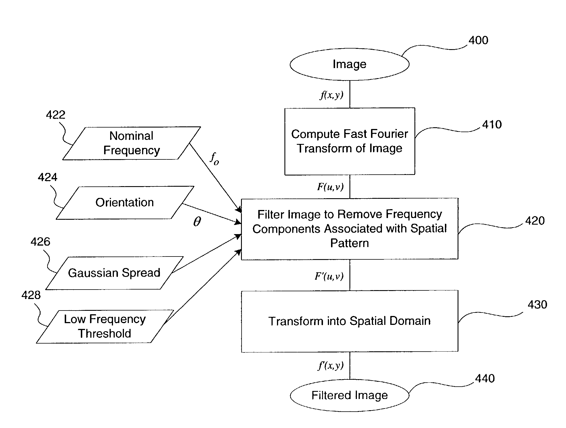
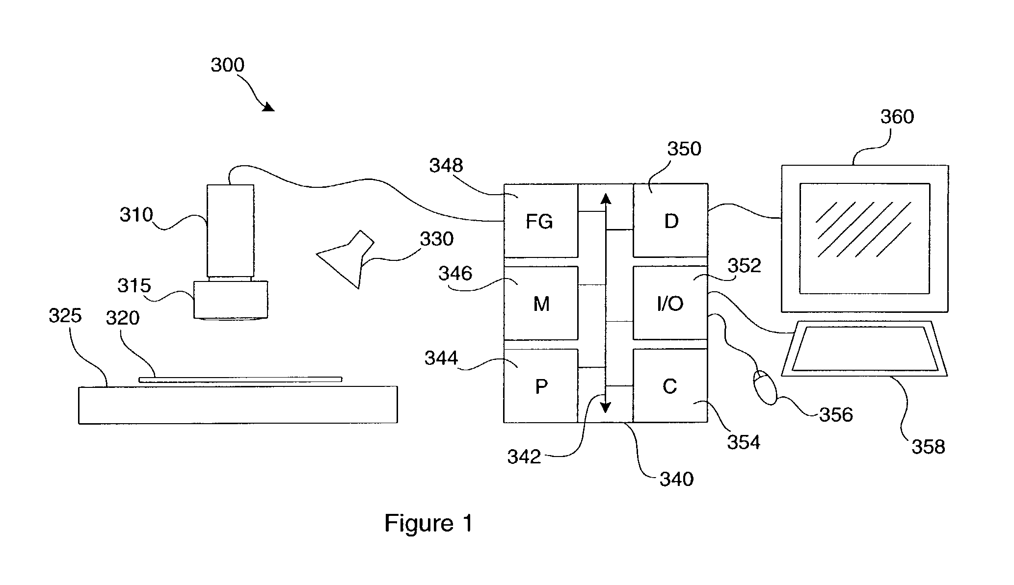
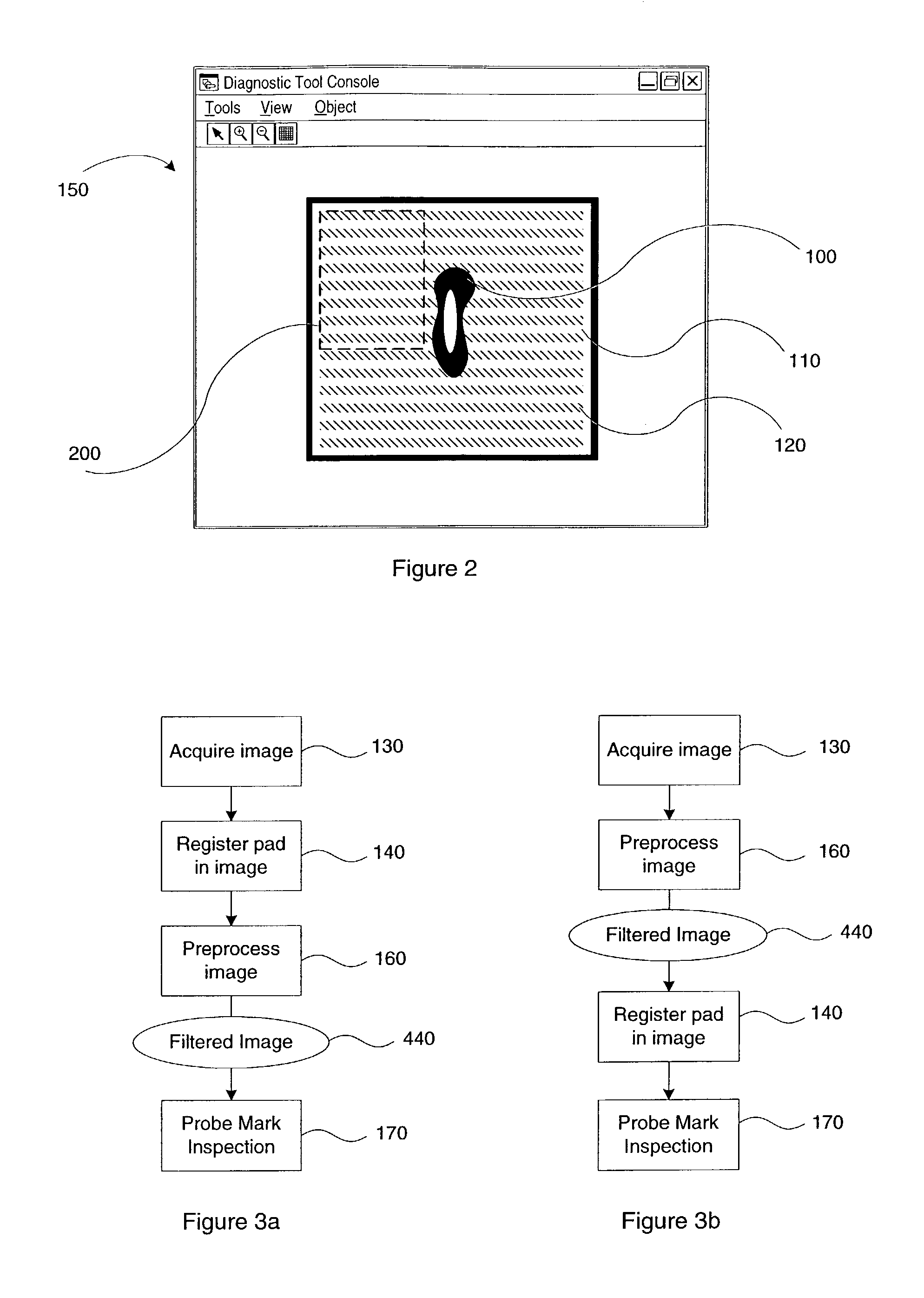
[0030]Probe mark inspection is typically performed during silicon device fabrication to inspect for, and report characteristics of, the marks made on the surface of the silicon device interconnection pads by an electrical testing operation. The inspection can be performed using, for example, a machine vision inspection apparatus such as that commonly used in semiconductor device manufacturing, as depicted in FIG. 1. Referring to FIG. 1, the inspection apparatus 300 may include an image acquisition system comprising a camera 310 having a lens 315 cooperative to provide an image of the surface of a semiconductor wafer 320. The wafer 320 can be mounted on a translation table 325 to permit adjustment of the position of the wafer 320 relative to the camera 310. An illumination device 330 can be provided to sufficiently illuminate the surface of the wafer 320 for providing a quality image of the wafer 320.

[0031]The inspection apparatus 300 may include a machine vision system comprising a ...


PUM


Abstract

Digital image processing methods are applied to an image of a semiconductor interconnection pad to preprocess the image prior to an inspection or registration. An image of a semiconductor pads exhibiting spatial patterns from structure, texture or features are filtered without affecting features in the image not associated with structure or texture. The filtered image is inspected in a probe mark inspection operation.

Description

CROSS-REFERENCE TO RELATED APPLICATIONS[0001]This application claims the benefit of U.S. Provisional Patent Application No. 60 / 382,896, filed May 22, 2002, entitled “Image Processing for Probe Mark Inspection.”BACKGROUND OF THE INVENTION[0002]The present invention relates to the application of machine vision algorithms in the manufacture of semiconductor devices. Specifically, the invention applies to the inspection of interconnection lands, or pads, of integrated circuits during fabrication, to ascertain that mechanical probe marks exist, indicating that an electrical test has been performed. The use of an inspection apparatus that can automatically detect and analyze probe marks on device lands can be more reliable and accurate than manual inspection with the human eye.[0003]Silicon device fabrication involves various circuit definition steps with chemical processing of a wafer containing an array of multiple devices. An electrical test of the wafer is typically employed to identi...

Claims


Application Information

Patent Timeline
IPC IPC(8): G06K9/34
CPCG06T5/002G06T5/10G06T5/20G06T7/0004G06T2207/20056G06T2207/30148
Inventor WALLACK, AARONKOLJONEN, JUHAMICHAEL, DAVID
Owner COGNEX TECH & INVESTMENT
Why Eureka
Try Eureka