Low power memory controller that is adaptable to either double data rate DRAM or single data rate synchronous DRAM circuits

a memory controller and low power technology, applied in the field of low power memory controllers, can solve the problems of inability to easily adapt the memory controller to accommodate, the cost of making ddr on a per-byte basis might also steadily decline compared to the sdr counterpart, and the existing memory controllers formed on an integrated circuit with an execution engine cannot be readily adapted to either form of memory

Active Publication Date: 2007-07-10
AVAGO TECH INT SALES PTE LTD
View PDF6 Cites 40 Cited by
  • Summary
  • Abstract
  • Description
  • Claims
  • Application Information

AI Technical Summary

Benefits of technology

[0014]The problems outlined above are in large part solved by an improved memory controller. The memory controller hereof can be used to control various types of DRAM, such as SDR or DDR DRAM. The memory can be embedded on the same PCB as the memory controller or, alternatively, the memory can be placed on a separate PCB, such as a SIMM or DIMM. In either instance, the memory controller can accommodate SDR or DDR DRAM memory types, such as SDR SDRAM or DDR DRAM without any modification to the memory controller hardware. Thus, users can simply “plug-and-play” different types of DRAM memory into the computing system without having to modify the execution engine or the memory controller. This implies that the execution unit and memory controller can be arranged on a common integrated circuit, as an ASIC, PLA, etc. As the market changes and the costs associated with one type of memory makes DDR DRAM more attractive than, for example, SDR SDRAM, a user can simply replace the SDR SDRAM with DDR DRAM without making any changes to the integrated circuit which bears the execution unit and memory controller.

Problems solved by technology

However, it is typically difficult to easily modify the memory controller to accommodate, for example, SDRAM instead of DRAM.
As the market demand for higher speed DDR increases, the costs associated with making DDR on a per-byte basis might also steadily decline compared to the SDR counterpart.
Yet, existing memory controllers formed on an integrated circuit with an execution engine cannot be readily adapted to either forms of memory, either because the memory controller is fixed in its ASIC design or the functionality of the memory controller suited for SDR cannot be readily modified to accommodate, for example, the DQS signals and latching on both the rising and falling clock edges.

Method used


Image

  • Low power memory controller that is adaptable to either double data rate DRAM or single data rate synchronous DRAM circuits
  • Low power memory controller that is adaptable to either double data rate DRAM or single data rate synchronous DRAM circuits
  • Low power memory controller that is adaptable to either double data rate DRAM or single data rate synchronous DRAM circuits

Examples


Embodiment Construction

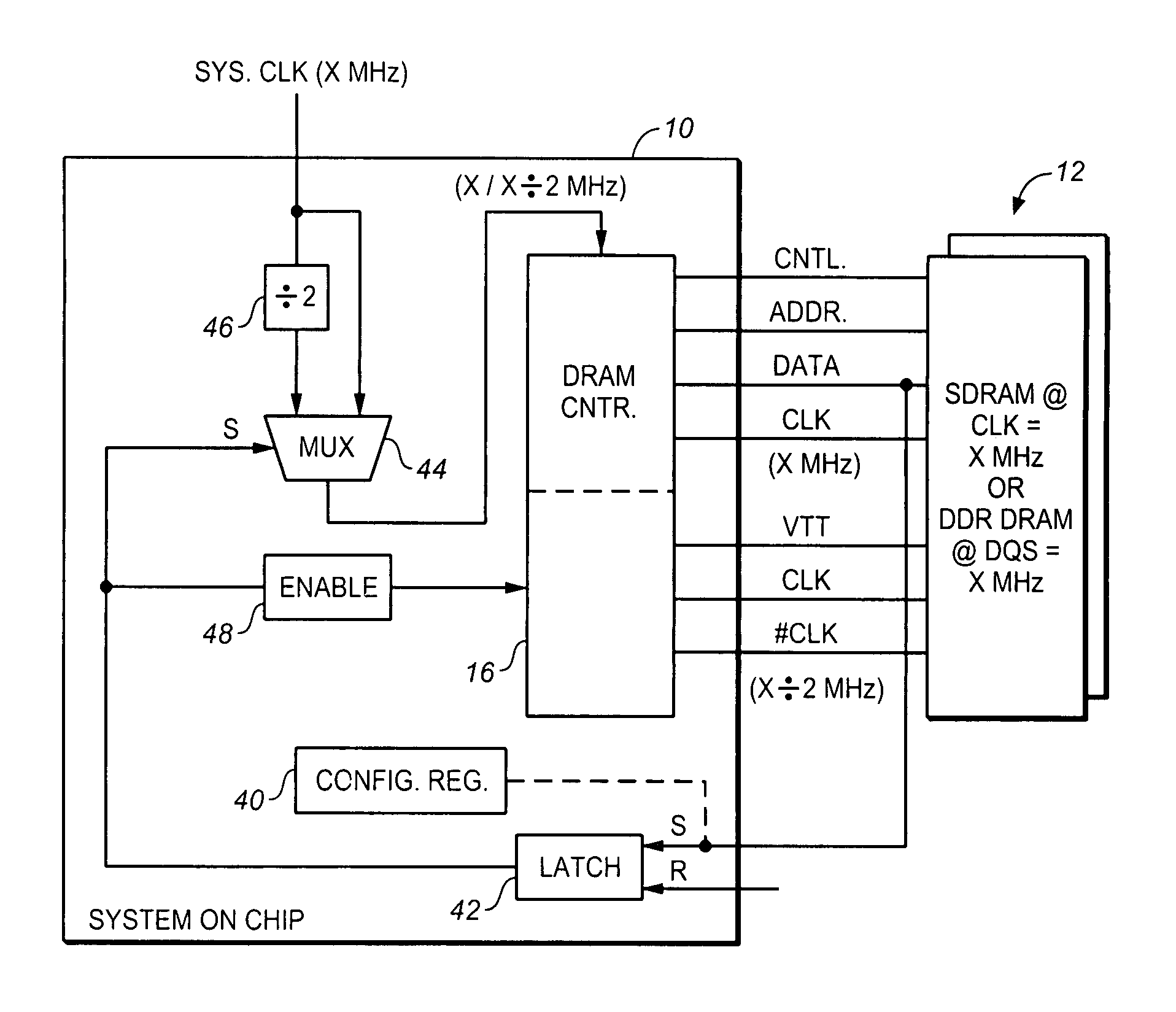
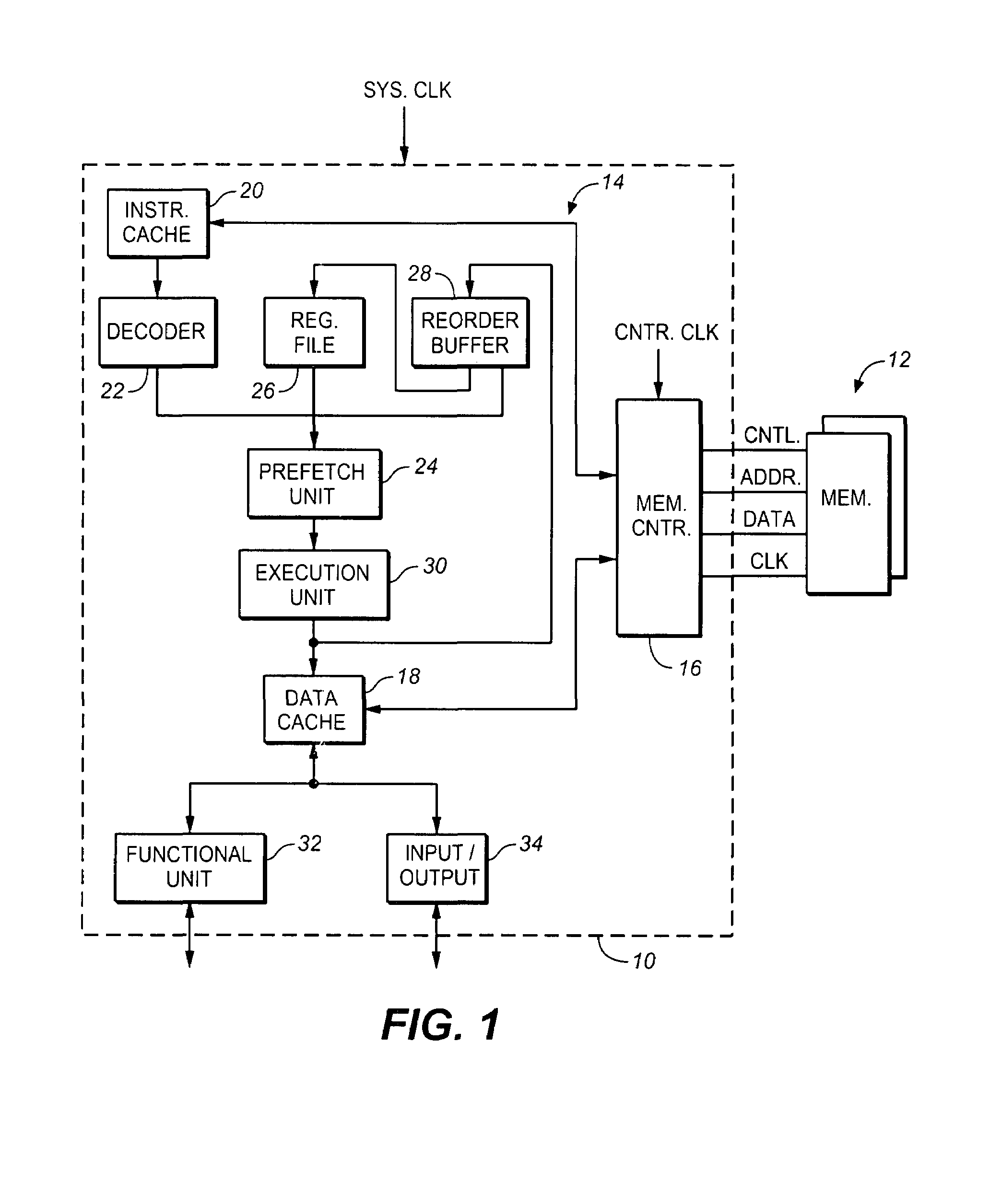
[0030]Turning now to the drawings, FIG. 1 illustrates a block diagram of various functional blocks within an integrated circuit 10 connected to external memory 12. External memory 12 is shown having several input / output pins, some of which are reserved for control, address, data, and clock pins that are coupled to pins of memory 12 via, for example, trace conductors within a substrate, such as a PCB. Within integrated circuit 10 are essentially two major subsystems: an execution engine 14 and a memory controller 16.

[0031]Execution engine 14 is illustrated in part. Preferably, execution engine 14 is a processor. A processor is known to incorporate two operational units: an integer unit and a floating-point unit. These units communicate data via a data cache 18 drawn from, for example, external memory 12. The integer and floating-point units are controlled by a single instruction stream supplied by instruction cache 20. The instruction stream can be drawn from external memory 12, for ...


PUM


Abstract

A memory controller is provided and a method for transferring data between the memory controller and a memory device. The memory controller can be implemented on an integrated circuit that also contains an execution unit. The execution unit can be clocked at a first clock rate, whereas the memory controller can be selectively clocked at either the first clock rate or a second clock rate that is approximately one-half frequency of the first clock rate. By clocking the memory controller at either the first clock rate or the second clock rate, the memory controller can accommodate different types of semiconductor memory. For example, the memory controller can control single data rate (SDR) DRAM memory if it is clocked at a first clock rate. Conversely, the memory controller can control double data rate (DDR) DRAM memory if it is clocked at approximately one-half the first clock rate. By selectively clocking the memory controller at different clocking rates, the memory controller need not be modified in hardware, yet can accommodate different memory devices by allowing a user to simply plug one type of memory into a receptacle rather than another depending on the cost constraints and user application. Therefore, the memory controller is adaptable during a power-on reset in which the computer system is initialized to automatically receive and control different types of memory selected by a user.

Description

BACKGROUND OF THE INVENTION[0001]1. Field of Invention[0002]This invention relates to semiconductor memory and, more particularly, to a low power memory controller embodied upon an integrated circuit for selectively controlling either a single data rate (SDR) synchronous dynamic random access memory (SDRAM) or a double data rate (DDR) DRAM.[0003]2. Description of Related Art[0004]The following descriptions and examples are not admitted to be prior art by virtue of their inclusion within this section.[0005]There are numerous types of memories available in the marketplace. For example, large volumes of data can be stored in magnetic memory, such as a hard disk drive. Lesser quantities of data can be stored in memory arranged upon an integrated circuit, oftentimes referred to as “semiconductor memory.” Semiconductor memory is typically arranged closer to the core logic unit or execution unit (oftentimes referred to as the “execution engine”) than the hard disk drive, and can be accesse...

Claims


Application Information

Patent Timeline
Patent Type & Authority Patents(United States)
IPC IPC(8): G06F1/04
CPCG06F13/1694
Inventor KUROODI, VIJENDRADESAI, GEETAHUNG, ERIC
Owner AVAGO TECH INT SALES PTE LTD
Why Eureka
Try Eureka