
Semiconductor device with improved wiring arrangement utilizing a projecting portion and a method of manufacturing the same

a technology of projecting portion and semiconductor device, which is applied in the direction of semiconductor device, semiconductor/solid-state device details, electrical apparatus, etc., can solve the problems of deteriorating wiring efficiency (wiring mounting efficiency), and achieve the effects of improving connection accuracy, improving wiring mounting efficiency, and high density

Inactive Publication Date: 2007-07-17
HITACHI LTD
View PDF3 Cites 9 Cited by
  • Summary
  • Abstract
  • Description
  • Claims
  • Application Information

AI Technical Summary

Benefits of technology

[0010]It is an object of the present invention to improve the wiring mounting efficiency and also improve the connection accuracy between wirings.

Problems solved by technology

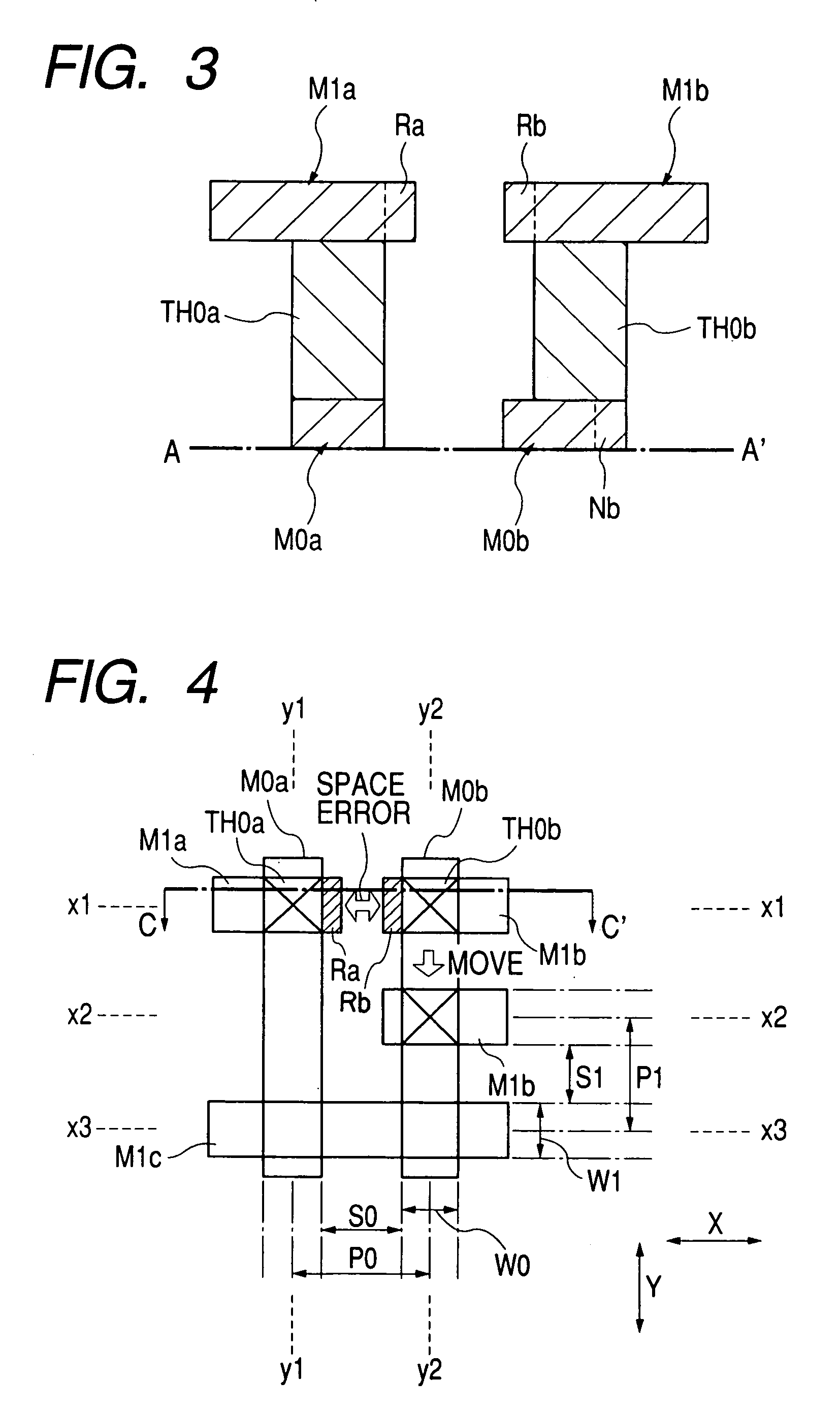
However, in a layout which does not cause a wiring error in the absence of a reservoir, there occurs a wiring rule error (violation) in the presence of a reservoir, thus giving rise to the problem that the wiring efficiency (wiring mounting efficiency) is deteriorated, as will be described in detail later.

Method used


Image

  • Semiconductor device with improved wiring arrangement utilizing a projecting portion and a method of manufacturing the same
  • Semiconductor device with improved wiring arrangement utilizing a projecting portion and a method of manufacturing the same
  • Semiconductor device with improved wiring arrangement utilizing a projecting portion and a method of manufacturing the same

Examples


first embodiment

[0054]With reference to the drawings, a description will be given below of a method for disposing wirings, etc. in a semiconductor device of this first embodiment.

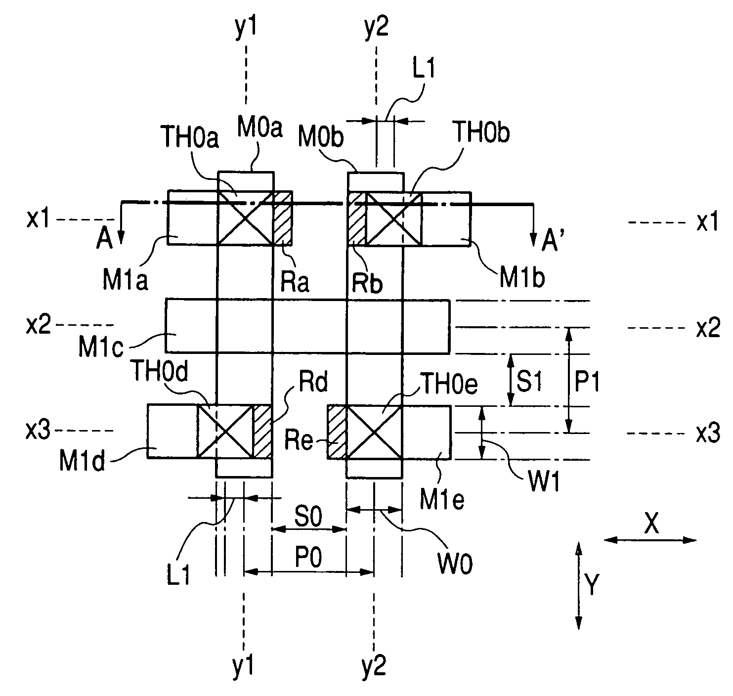
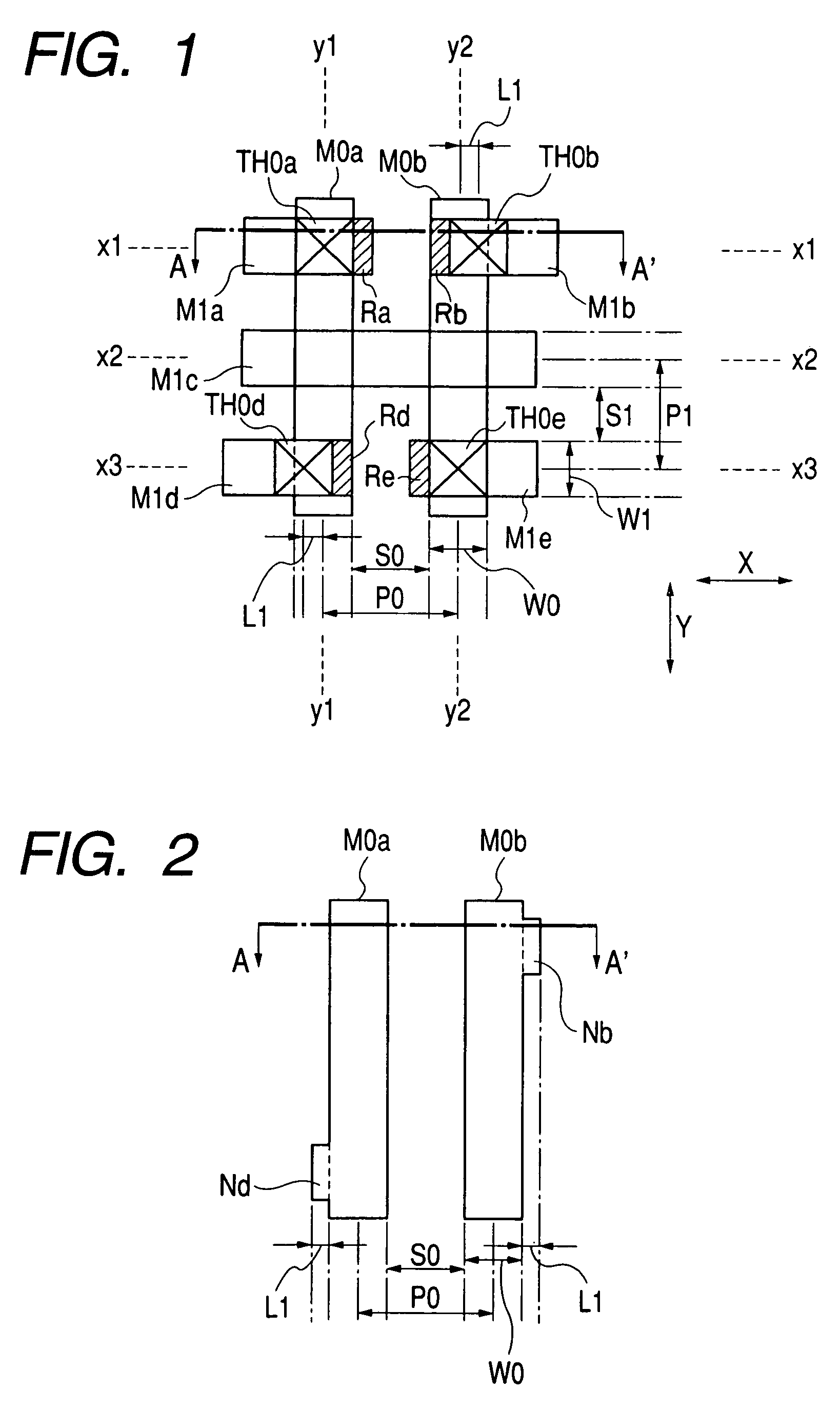
[0055]FIG. 1 is a plan view showing planar patterns 0th layer wirings M0a, M0b, first layer wirings M1a˜M1e, and connections TH0a, TH0b between the 0th and the first layer wirings; FIG. 2 illustrates planar patterns of the 0th wirings M0a and M0b in the layout of FIG. 1; and FIG. 3 is a sectional view of principal portions taken on line A–A′ in FIG. 1. An interlayer insulating film is present between wirings.

[0056]The following description is directed to the state of the wirings, etc. which are disposed in the semiconductor device of this embodiment.

[0057]Oth layer wirings M0a and M0b are disposed along grids (layout lines, channels) y1 and y2 which extend in the Y direction. The grids consist of lines which are defined at equal intervals in the X or Y direction and which define a minimum wiring spacing between layers. The...

second embodiment

[0093]A semiconductor device is designed by utilizing a computer (CAD). CAD is essential for a short-period development of LSI (Large Scale Integrated Circuit). A computer system (CAD system) used for CAP is constituted by a group of CAD tools, which are used according to various design steps. In other words, the CAD tools are software programs developed for a specific purpose. Thus, the wirings described in the first embodiment can also be laid out automatically using a CAD tool.

[0094]The following description is directed to a CAD tool (automatic wiring tool) for realizing the wiring layout described in the first embodiment. The shape, etc. of wirings laid out using CAD tools in this second embodiment are the same as in the layout which has been described above with reference to FIG. 1, etc. in connection with the first embodiment, so that the details thereof will be omitted.

[0095]As described in the first embodiment, there are various conditions for the layout of wiring. a) The 0t...

third embodiment

[0112]Although in the first embodiment only the connection TH0b, of the connections TH0a and TH0b that are disposed adjacent to each other, is disposed offsetwise (see FIG. 1), the adjacent connections TH0a and TH0b may be displaced in directions opposite to each other (away from each other).

[0113]With reference to the drawings, a description will be given below of a method for disposing wirings, etc. in the semiconductor device of this embodiment. This third embodiment is the same as the first embodiment, except for the layout positions of connections and first layer wirings, so that corresponding portions are identified by the same reference numerals, and only different portions will be described in detail below.

[0114]FIG. 12 is a plan view showing planar patterns of 0th layer wirings M0a, M0b, first layer wirings M1a to M1e, and connections TH0a and TH0b between the 0th and the first layer wirings. FIG. 13 illustrates planar patterns of the 0th layer wirings M0a and M0b in the la...


PUM


Abstract

In a method of manufacturing a semiconductor device having a first wiring extending in a first direction and a second wiring connected to the first wiring through a connection and extending in a second direction orthogonal to the first direction, the second wiring having a surplus portion projecting from the connection in a direction opposite to the second direction, the first and second wirings are arranged such that a center of the connection is offset in the second direction from a center of the first wiring, and a projecting portion of the first wiring is disposed under the connection.

Description

BACKGROUND OF THE INVENTION[0001]The present invention relates to a semiconductor device and a method of manufacturing the same. More particularly, the invention is concerned with a technique which is effective in the formation of a connection of wirings between different layers.[0002]A semiconductor element and wiring, or wirings of different layers, are interconnected through a conductive film formed within a connecting hole. However, with microstructurization of semiconductor devices, studies are being made concerning a technique in which a portion, called a reservoir, is provided in an upper-layer wiring which overlies a connection. This technique is used for the following reason.[0003]The reservoir represents a projecting portion (a surplus portion, a marginal portion) which is a part of the wiring and which projects from a wiring portion serving as a main current path. Although such a reservoir portion represents an unnecessary portion as a current path, it is formed for impro...

Claims


Application Information

Patent Timeline
IPC IPC(8): H01L23/52H01L21/3205H01L21/768H01L21/82H01L21/822H01L21/8234H01L23/528H01L27/04H01L27/088H01L27/118
CPCH01L23/528H01L27/118H01L2924/0002H01L2924/00H01L21/82
Inventor MURATA, TOMOOYABUKI, SHINOBUYAMASHITA, TAKEO
Owner HITACHI LTD
Learn More