Sample-hold circuit
a sample-holding circuit and sample-holding technology, applied in the field of sample-holding circuits, can solve the problems of increasing power consumption, aggravated droop, and restricting design parameters, and achieves the effects of reducing droop, wide design freedom, and high speed
- Summary
- Abstract
- Description
- Claims
- Application Information
AI Technical Summary
Benefits of technology
Problems solved by technology
Method used
Image
Examples
first embodiment
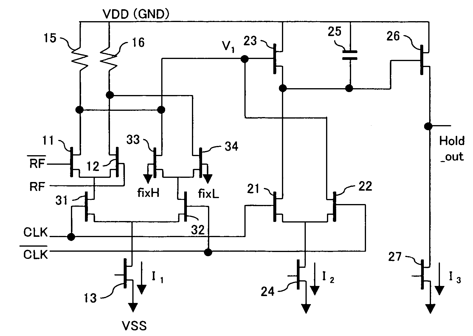
[0031]FIG. 4 is the principle configuration block diagram of a sample-hold circuit according to the present invention. This diagram shows the principle configuration of the sample-hold circuit comprising a preamplifier 1 to which the input analog signal is applied and corresponds to the sample-hold circuit according to the present invention, later described.
[0032]In FIG. 4, the amplified output of the input analog signal from the preamplifier 1 is applied as an input to a core section 2 which outputs a voltage corresponding to the variation in the input analog signal during the sampling period, holds the value of the voltage corresponding to the amplified output at the time of transition of the sample clock signal, and outputs the held value during the hold period.
[0033]The current switching circuit 3 is connected to the output pin of the preamplifier and enables the current flowing into the first transistor comprised within the preamplifier 1 during the sampling period to flow into...
second embodiment
[0037]The sample-hold circuit which partially corresponds to the sample-hold circuit later described comprises a preamplifier to which the input analog signal is applied and a core section to which the output of the preamplifier is applied, as in FIG. 4. In addition, the core section of the sample-hold circuit is comprised of first and second transistors, which are connected in series and to each gate of which the sample clock signal is applied, and a capacitance which is connected to one of the first and second transistors and holds the value of the voltage corresponding to the output of the preamplifier at the time of the transition of the sample clock signal.
[0038]Similarly, another sample-hold circuit, which partially corresponds to the second embodiment, described later, comprises a preamplifier and a core section. The core section comprises a capacitance which holds the value of the voltage corresponding to the output of the preamplifier at the time of the transition of the sa...
third embodiment
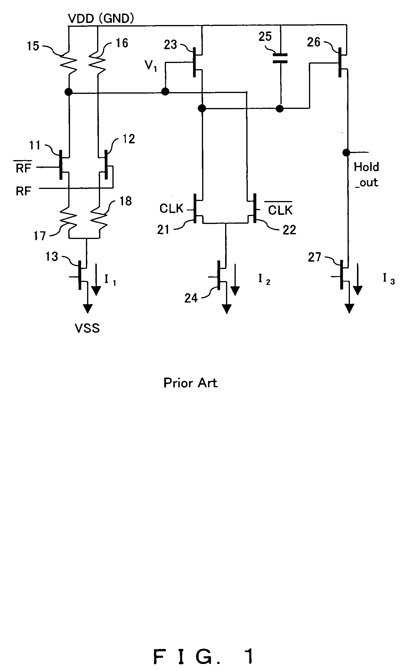
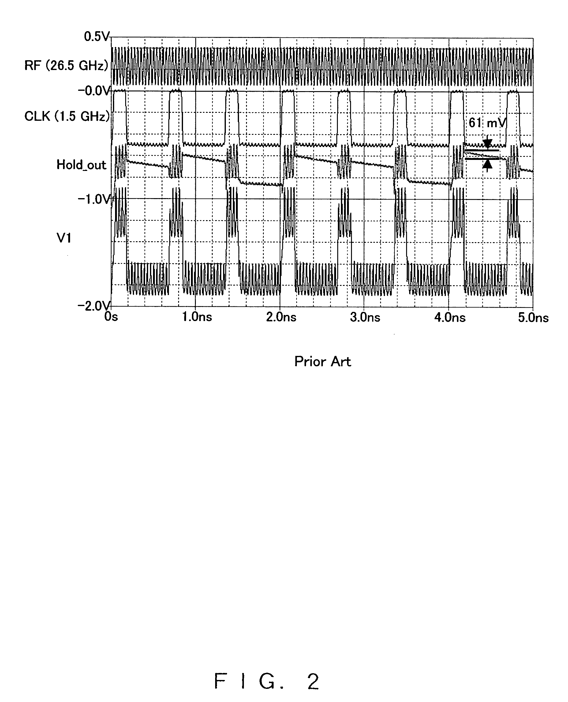
[0062]FIG. 10 is the simulation result of the third embodiment in FIG. 7. The maximum value of the droop is 33 mV, and it can be understood that the droop is improved by 46%, compared to that in FIG. 2. In addition, the improvement effect on the feed through is evident.
PUM
 Abstract
Description
Claims
Application Information


