

Charge pump circuit with dynamic biasing of pass transistors
a charge pump and transistor technology, applied in the field of two-phase, can solve the problems of unavoidable loss of output voltage, increased drawback, and increased charge pump stage number
- Summary
- Abstract
- Description
- Claims
- Application Information
AI Technical Summary
Benefits of technology
Problems solved by technology
Method used
Image

Examples
Embodiment Construction
[0021]Preferred embodiments of the present invention will be described in detail hereinbelow with reference to the attached drawings.
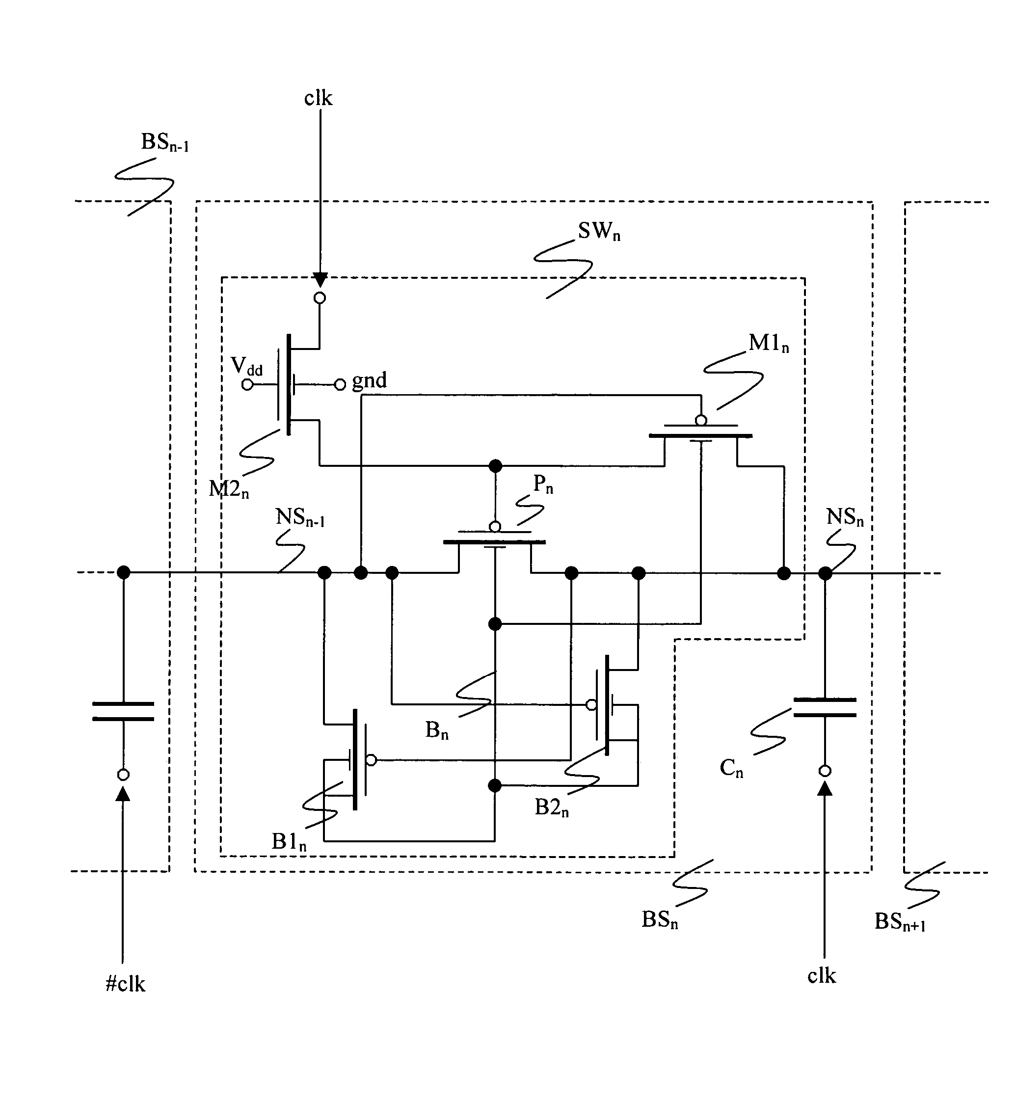
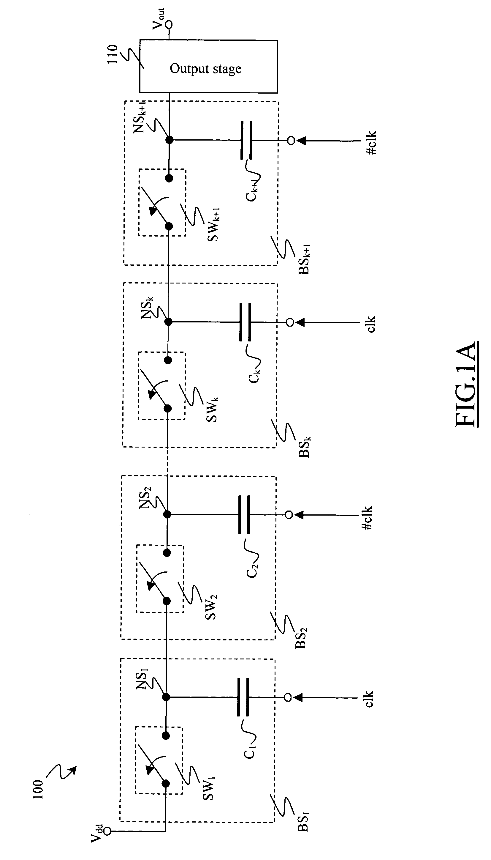
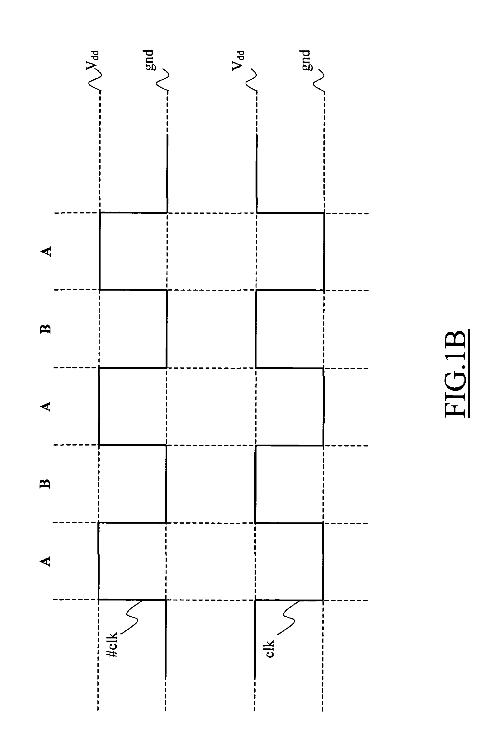
[0022]One preferred embodiment of the present invention provides a two-phase charge pump, which is suitable to be controlled by a first clock signal and a second clock signal. Each clock signal periodically has a first value and a second value during a first phase and a second phase, respectively; the first and the second clock signals are in phase-opposition. The charge pump has a sequence of cascade-connected stages. Each stage includes a capacitive element that is driven by a corresponding one of the clock signals; the capacitive elements of each pair of adjacent stages are driven by different clock signals. A pass transistor is used for transferring electric charge to the capacitive element of the stage from the capacitive element of a previous stage. The stage further includes a first biasing circuit for enabling the pass transistor during the fir...
PUM
 Abstract
Description
Claims
Application Information