
Organic light emitting diode display having shield electrodes

a light-emitting diode and shield electrode technology, applied in the field of display devices, can solve the problems of reducing the size of pixels, adding to the total power consumption of the display, and high leakage current, and achieve the effect of enhancing the performance of the display and minimizing parasitic capacitan

Inactive Publication Date: 2007-07-24
IGNIS INNOVATION
View PDF4 Cites 226 Cited by
  • Summary
  • Abstract
  • Description
  • Claims
  • Application Information

AI Technical Summary

Benefits of technology

[0020]It is an object of the present invention to provide a polymeric or organic light emitting diode(OLED) display having shield electrodes for minimizing parasitic capacitances to enhance the performance thereof.
[0021]It is another object of the present invention to provide an OLED display having shield electrodes for allowing surface emission through vertical pixel circuitry integration for a high aperture ratio.
[0027]The OLED display with the above structure according to the present invention minimizes parasitic capacitance in the drive circuit and leakage currents in the thin-film transistors by holding the voltage at the gate of the driver thin-film transistor.
[0028]Further, the OLED display according to the present invention allows the OLED layer to be vertically stacked on the backplane electronics, along with a transparent top electrode for the top or surface emission.

Problems solved by technology

The same problem happens when pixel sizes are scaled down.
However, the continuous back electrode can give rise to parasitic capacitance causing the leakage current of the transistor T1, whose effects can become significant enough to affect the operation of the driver transistor T2 when the continuous back electrode runs over the switching and other thin film transistors.
That is, the presence of the continuous back electrode can induce a parasitic channel in thin-film transistors giving rise to high leakage current.
Accordingly, it adds to the total power consumption of the display.

Method used


Image

  • Organic light emitting diode display having shield electrodes
  • Organic light emitting diode display having shield electrodes
  • Organic light emitting diode display having shield electrodes

Examples


Embodiment Construction

[0039]Hereinafter, descriptions will be made in detail on an organic light emitting diode display according to the embodiments of the present invention with reference to the accompanying drawings. Like reference numerals denotes like constituents throughout the disclosure.

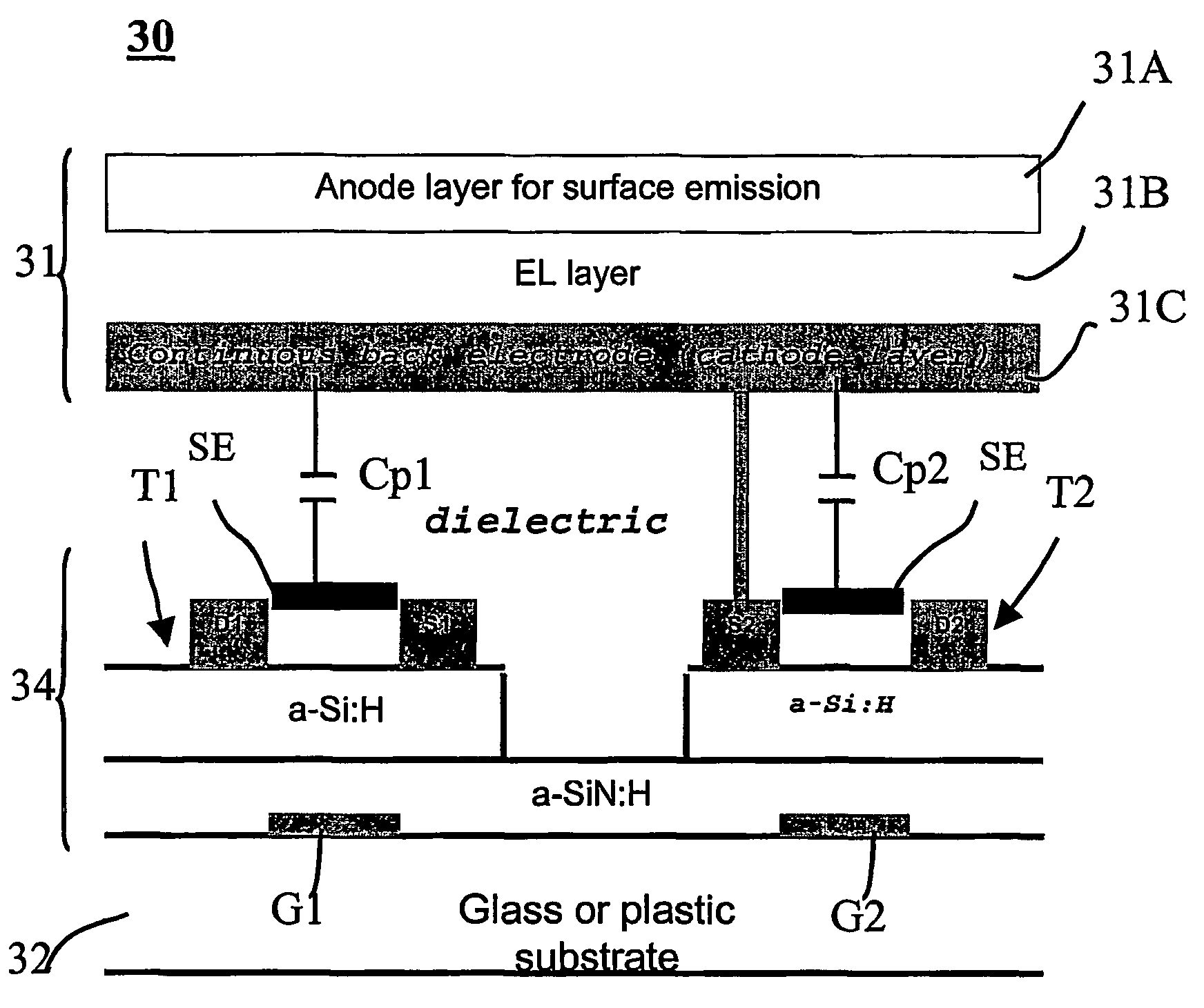
[0040]FIG. 3 is a cross-sectioned view for showing a pixel of an AMOLED display with shield electrodes formed over a drive circuit according to an embodiment of the present invention.

[0041]As stated above, the AMOLED display consists of a matrix array of pixels, but FIG. 3 shows only one pixel for the sake of simplicity in description.

[0042]As shown in FIG. 3, a pixel 30 includes an OLED layer 31, intermediate or shield electrodes SE, a drive circuit 34, and a substrate 32.

[0043]The OLED 31 has an anode electrode or an anode layer 31A, an EL layer 31B, and a cathode layer 31C. FIG. 3 shows the top or surface emission pixel. The cathode electrode 31C forms a continuous back electrode.

[0044]The drive circuit 34 consi...


PUM


Abstract

An organic light emitting diode (OLED) display includes at least one shield electrode between a cathode layer and an OLED drive circuit. The OLED drive circuit has at least one thin-film transistor (TFT), and the shield electrode is disposed to correspond to the thin-film transistor and closer to the cathode layer, covering an entire region between the source and drain of the thin-film transistor. The shield electrode is either grounded or tied to the gate of the thin-film transistor, to thereby minimize parasitic capacitances in the pixels of the display to enhance the display performance. The presented architecture enables high density drive circuit integration in amorphous silicon or other technologies, yet preserving a high display aperture ratio.

Description

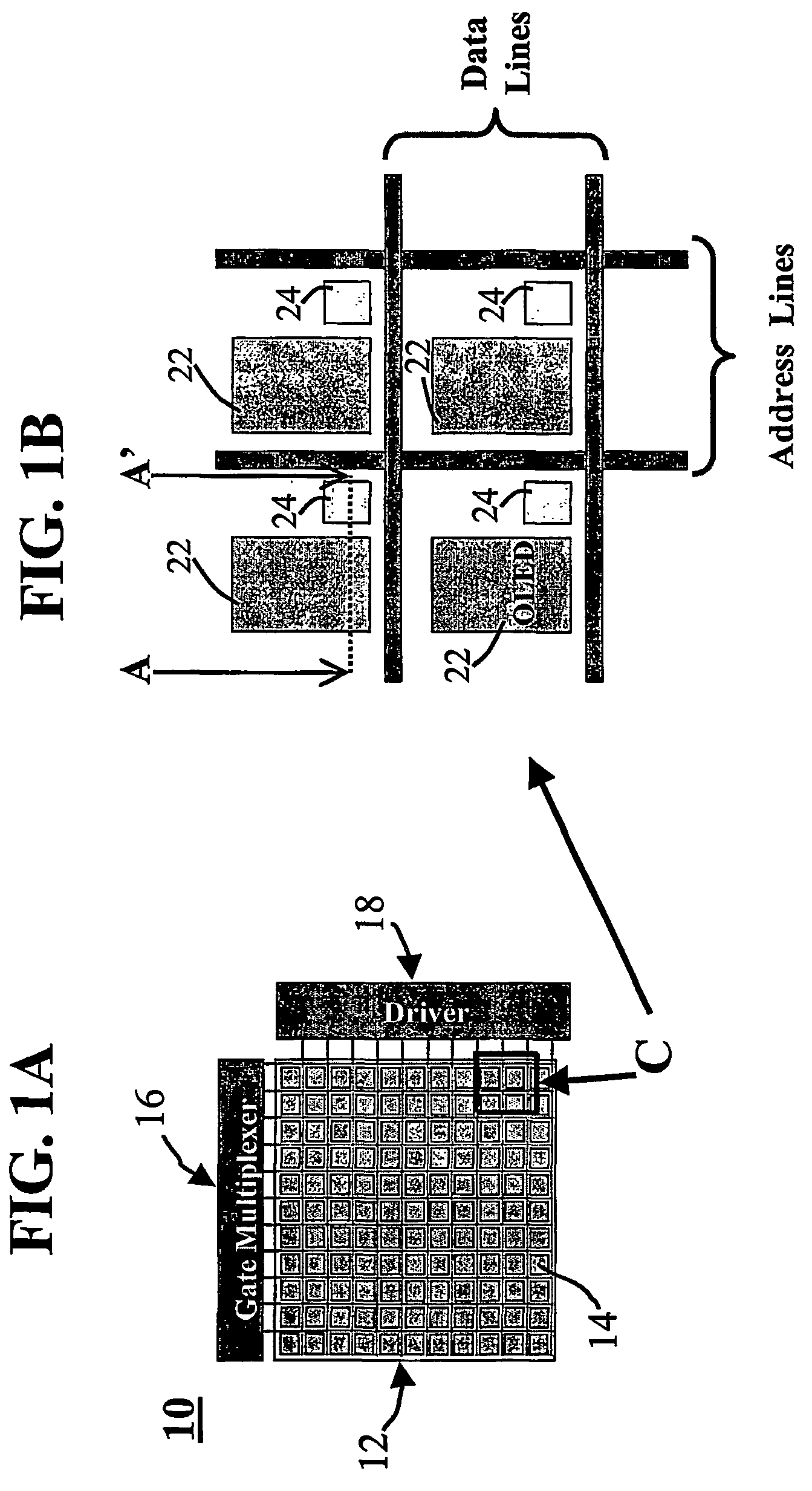
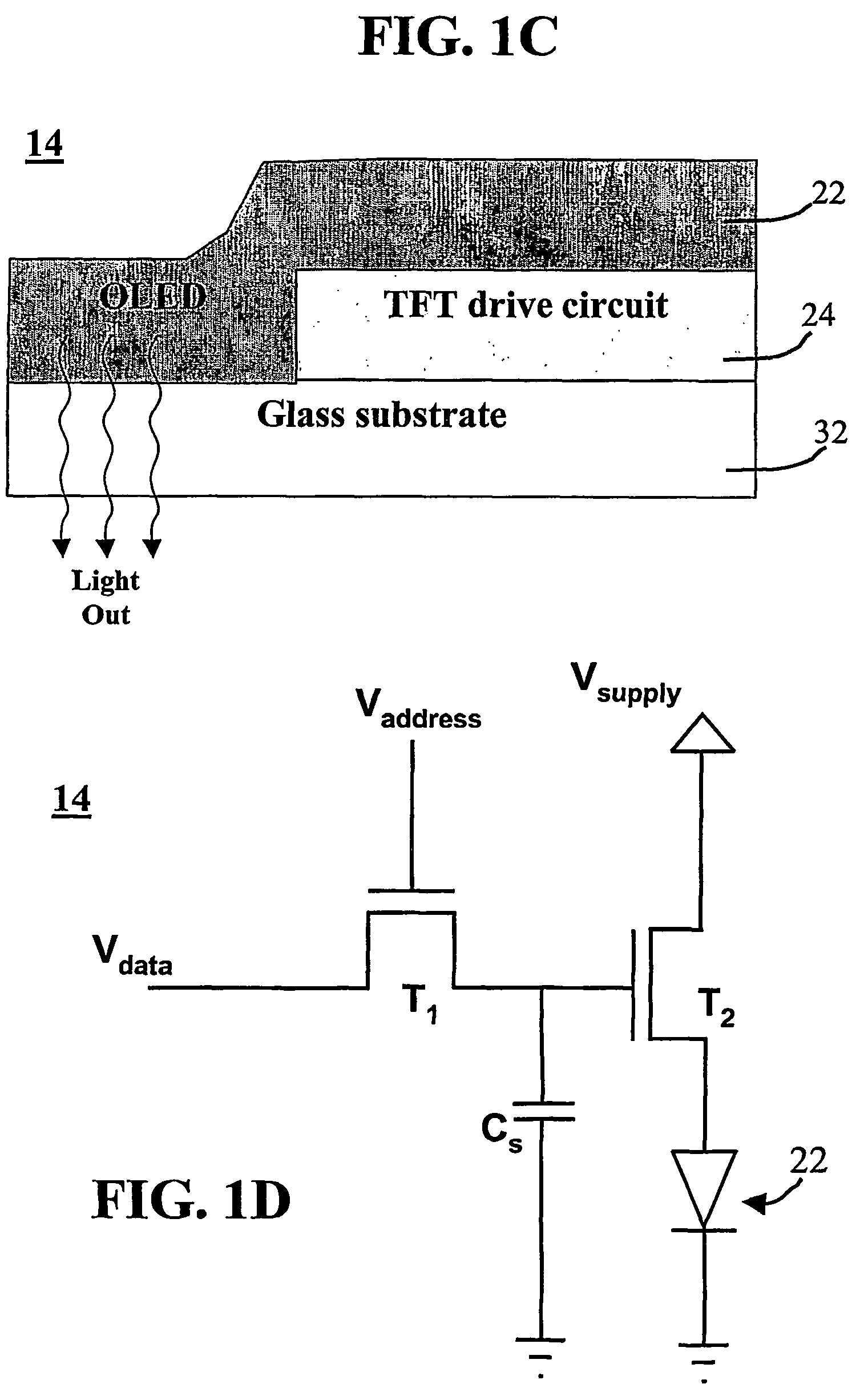
BACKGROUND OF THE INVENTION[0001]1. Field of the Invention[0002]The present invention relates to a display device, and more particularly to an organic light emitting diode display having shield electrodes.[0003]2. Description of the Prior Art[0004]The polymeric or organic light emitting diodes (OLEDS) are electroluminescent(EL) layers that emit light generated by radiative recombination of injected electrons and holes within one or more organic EL layers or an organic EL region thereof.[0005]The OLED displays employing the OLED have been attracting more attention because of their various advantages including simple structures, fast response times and wide viewing angles.[0006]FIG. 1A is a top view of a general active matrix OLED(AMOLED) display device. In FIG. 1A, a reference numeral 10 denotes an OLED display device. The OLED display device 10 has an OLED display 12, a gate multiplexer 16, and a driver 18. The OLED display 12 consists of a plurality of pixels 14 in a matrix array f...

Claims


Application Information

Patent Timeline
IPC IPC(8): G09G3/30G09G3/36H01L51/50G09F9/30H01L21/336H01L21/77H01L27/12H01L27/15H01L27/32H01L29/786
CPCH01L27/12H01L27/3272H01L27/124H01L2251/5315H10K59/126H10K2102/3026
Inventor NATHAN, AROKIASERVATI, PEYMANKARIM, KARIM S.
Owner IGNIS INNOVATION
Learn More