Antenna and method of making the same

a technology of antenna and resonant element, applied in the field of antenna, can solve the problems of low loss of coaxial line or waveguide tube circuit, increased transmission loss of other circuits fabricated on a planar substrate, and thick, heavyweight and lengthy system

Active Publication Date: 2007-07-31
PANASONIC CORP
View PDF30 Cites 12 Cited by
  • Summary
  • Abstract
  • Description
  • Claims
  • Application Information

AI Technical Summary

Benefits of technology

[0015]In order to overcome the problems described above, a primary object of the present invention is to provide an antenna that can strike an overall best balance among various antenna parameters such as directivity, gain and efficiency according to the radio wave propagation environment.
[0016]Another object of the present invention is to provide an apparatus and method for designing an antenna with required antenna properties easily.

Problems solved by technology

Generally speaking, circuits using a coaxial line or a waveguide tube have a low loss but often make a thick, heavyweight and lengthy system.
On the other hand, a microstrip circuit, a coplanar circuit and other circuits fabricated on a planar substrate tends to have an increased transmission loss but are flat, small-sized and lightweight.
There is often a radio wave obstruction such as something shielding or reflecting the radio wave between a mobile communications terminal station and a base station.
Besides, the radio wave propagation environment frequently changes in a complicated manner due to the shift of the location of such a radio wave obstruction or mobile communications terminal station.
That is why it is difficult to change those various antenna properties dynamically in response to any change in radio wave propagation environment.

Method used


Image

  • Antenna and method of making the same
  • Antenna and method of making the same
  • Antenna and method of making the same

Examples


embodiment 1

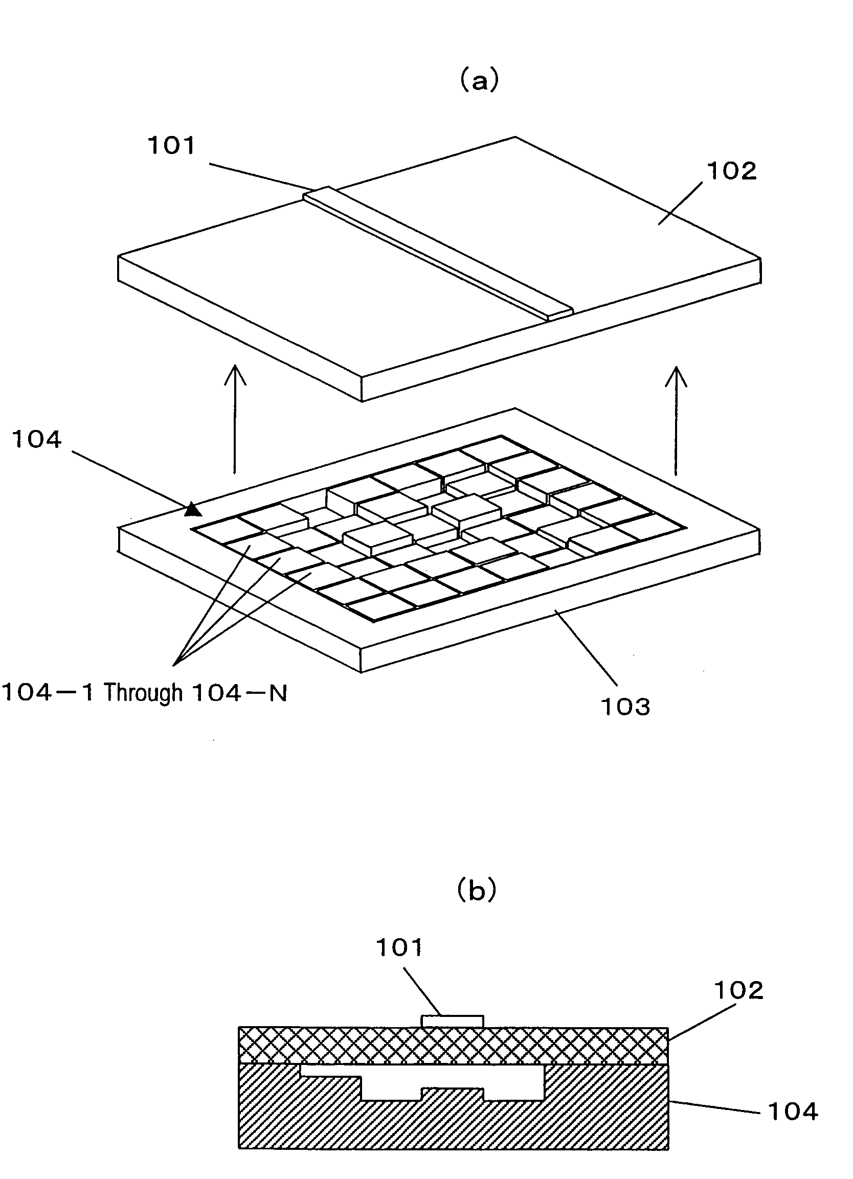
[0066]First, a first preferred embodiment of an antenna according to the present invention will be described with reference to FIGS. 1(a) and 1(b). FIGS. 1(a) and 1(b) are respectively an exploded perspective view and a cross-sectional view illustrating the antenna of this preferred embodiment.

[0067]As shown in FIGS. 1(a) and 1(b), the antenna of this preferred embodiment includes a dielectric layer 102, which has an upper surface (which will also be referred to herein as the “front side” on which a feeding line is provided) and a lower surface (which will be also referred to herein as the “backside” on which a grounded conductor is provided), a signal line strip (i.e., feeding conductor pattern) 101 arranged on the upper surface of the dielectric layer 102, a grounding conductor portion 104 arranged on the lower surface of the dielectric layer 102, and a supporting member 103 to support the grounding conductor portion 104.

[0068]The grounding conductor portion 104 of this preferred ...

example 1

[0087]Hereinafter, a specific example of an antenna according to the first preferred embodiment of the present invention will be described.

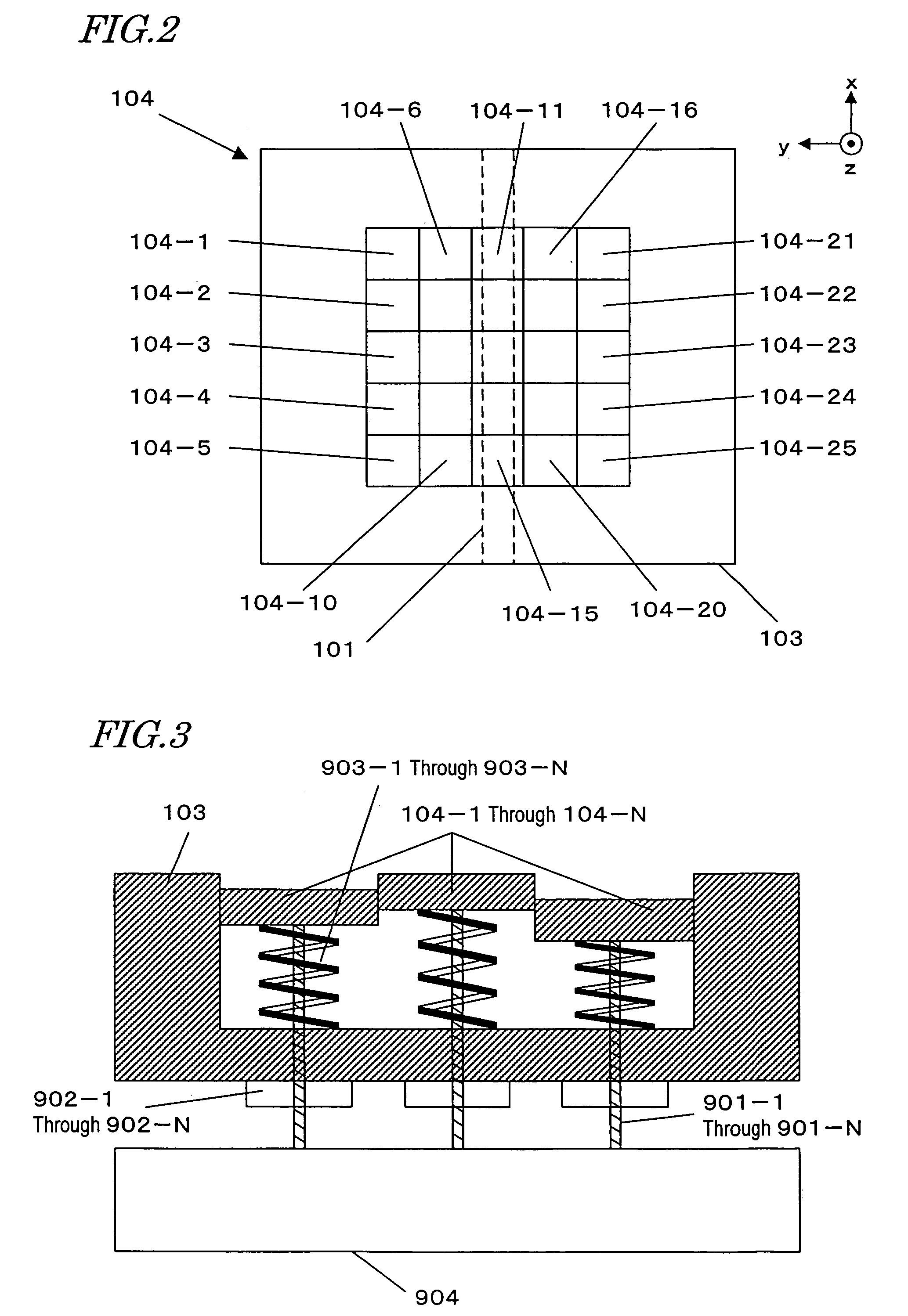
[0088]First, referring to FIGS. 6(a) and 6(b), illustrated are the displacement pattern of conductor elements of this specific example in FIG. 6(a) and a comparative example, in which the respective tops of the conductor elements (i.e., a plurality of planar areas included on the surface of the grounding conductor portion) are located at the same distance from a reference plane, in FIG. 6(b), respectively.

[0089]In this specific example, the respective conductor elements 104-1 through 104-N have a square upper surface with a size of 0.6 mm each side and are arranged in a 5×5 matrix pattern. Outside of the array of the conductor elements 104-1 through 104-N, there is a frame-shaped raised portion of the supporting member 103. A conductor layer has been deposited on the upper surface of this raised portion, which combines with the respective upper s...

example 2

[0098]Hereinafter, another specific example of an antenna according to the first preferred embodiment of the present invention will be described.

[0099]FIGS. 9(a) through 9(b) illustrate exemplary displacement patterns of grounding conductor elements 104-1 through 104-25 according to this specific example. In FIGS. 9(b) and 9(c), the position (i.e., the surface level) of the hatched conductor elements has shifted to a level that is 1.2 mm lower than-the reference plane. More specifically, in the example illustrated in FIG. 9(a), the surface of all conductor elements 104-1 through 104-25 is on a level with the reference plane and none of the conductor elements has been displaced at all. Accordingly, FIG. 9(a) shows a comparative example. On the other hand, in the examples illustrated in FIGS. 9(b) and 9(c), the surface of the eight or seven L-corner conductor elements has shifted to a level that is 1.2 mm lower than the reference plane, while the surface of the other conductor element...


PUM


Abstract

An antenna according to the present invention includes a dielectric layer 102 with an upper surface and a lower surface, a signal line strip 101 provided on the upper surface of the dielectric layer 102, and a grounding conductor portion 104 provided on the lower surface of the dielectric layer 102. The surface of the grounding conductor portion 104 includes a plurality of planar areas, each of which has a size that is shorter than the wavelength of an electromagnetic wave to transmit or receive. A distance from a virtual reference plane to each planar area is adjusted on an area-by-area basis. Thus, an antenna, which can change various antenna parameters such as radiation directivity, gain and efficiency dynamically and adaptively according to incessantly changing propagation environment of radio wave, is provided.

Description

[0001]This is a continuation of International Application PCT / JP2004 / 012249, with an international filing date of Aug. 19, 2004.BACKGROUND OF THE INVENTION[0002]1. Field of the Invention[0003]The present invention relates to an antenna for use in a wireless communication device that utilizes electromagnetic wave such as microwave or millimeter wave. The present invention can be used particularly effectively in a wireless LAN (local area network) used in office and homes and mobile communications terminals such as cell phones.[0004]2. Description of the Related Art[0005]Conventional RF circuits for use in wireless communication devices that utilize microwave to millimeter wave frequency bands include circuits that use a coaxial line or a waveguide tube and circuits that use a planar substrate. Generally speaking, circuits using a coaxial line or a waveguide tube have a low loss but often make a thick, heavyweight and lengthy system. On the other hand, a microstrip circuit, a coplanar...

Claims


Application Information

Patent Timeline
Patent Type & Authority Patents(United States)
IPC IPC(8): H01Q1/38H01Q1/24H01Q1/48H01Q3/01H01Q3/20H01Q9/04H01Q9/30H01Q13/08
CPCH01Q1/243H01Q1/38H01Q1/48H01Q3/01H01Q9/0407
Inventor FUJISHIMA, TOMOYASUSAKIYAMA, KAZUYUKISANGAWA, USHIOKANNO, HIROSHI
Owner PANASONIC CORP
Why Eureka
Try Eureka