Active-pixel image sensors

Active Publication Date: 2007-08-07
STMICROELECTRONICS SRL
View PDF3 Cites 12 Cited by
  • Summary
  • Abstract
  • Description
  • Claims
  • Application Information

AI Technical Summary

Benefits of technology

[0003]One object of the present invention is to redu

Problems solved by technology

However, the quality of images produced by active pi

Method used


Image

  • Active-pixel image sensors
  • Active-pixel image sensors
  • Active-pixel image sensors

Examples


Embodiment Construction

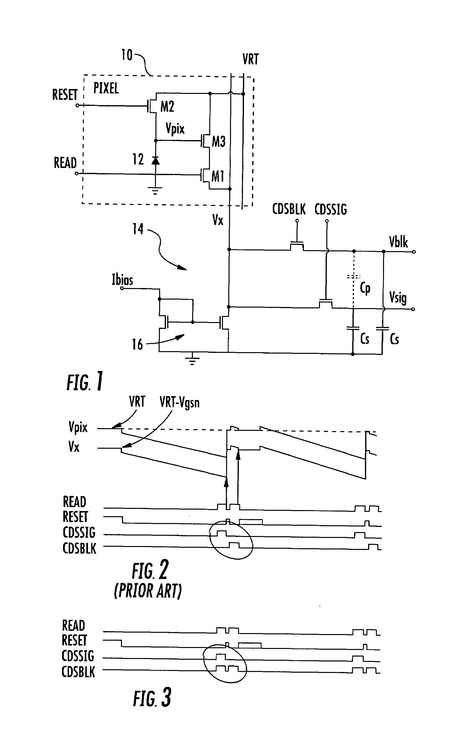
[0010]FIG. 1 shows one pixel 10 of a known three transistor pixel array. Each pixel comprises a photosensitive divide 12 and transistors M1, M2, M3. A reset voltage is supplied on line VRT, in this embodiment per column but horizontal VRT lines may also be used. Each column has an output circuit 14 connected to the column by line Vx and including double sampling capacitors Cs. A current source draws a current Ibias through the pixel source follower buffer amplifier 16.

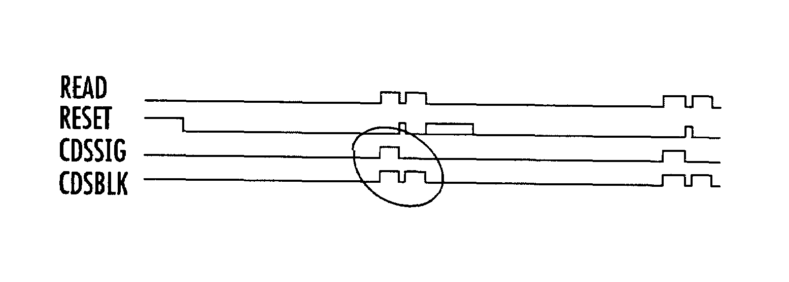
[0011]FIG. 2 shows the timing required to operate this circuit in a typical rolling shutter exposure mode. The pixel 10 voltage Vpix is periodically reset to the reference voltage VRT by pulsing reset high. When the pixel 10 is released from reset, it begins to integrate photogenerated current on the capacitance of the photodiode 12. The light signal is detected after a certain exposure time. The read signal goes high and the signal CDSSIG pulses, thus sampling the source follower output (Vpix−Vgsn) as Vsig, where Vgsn...


PUM


Abstract

An image sensor has an array of pixels read by column circuits to provide reset and read samples on a pair of sample capacitors. To alleviate the effects of parasitic capacitance in the region of the sample capacitors, a modified timing arrangement is used. Both sample switches are operated simultaneously to pre-charge both sample capacitors with a pixel signal value. One sample switch is operated after reset to apply a reset value to one of the pre-charged sample capacitors.

Description

FIELD OF THE INVENTION [0001]The present invention relates to active-pixel image sensors, and more particularly to CMOS image sensors.BACKGROUND OF THE INVENTION [0002]As is well known, active-pixel image sensors have the advantage that they can be made as single chips by conventional CMOS technology, in contrast to CCD image sensors which require special fabrication facilities and are typically implemented as multiple chips due to the range of power supplies required. However, the quality of images produced by active pixel CMOS sensors is poorer than that of CCD devices. One reason for this is the presence of fixed pattern noise (FPN), which includes pixel-to-pixel FPN and vertical FPN. FPN is particularly present when double sampling (sometimes referred to as correlated double sampling) is used to reduce other sources of noise.SUMMARY OF THE INVENTION [0003]One object of the present invention is to reduce FPN in active pixel double sampling image sensors.[0004]An image sensor has ...

Claims


Application Information

Patent Timeline
IPC IPC(8): H04N5/217H04N5/21H01L27/00H04N3/14H04N5/335H04N5/357H04N5/365
CPCH04N3/1568H04N5/3575H04N5/3653H04N25/616H04N25/672
Inventor HENDERSON, ROBERTHURWITZ, JONATHAN EPHRIAM DAVID
Owner STMICROELECTRONICS SRL
Why Eureka
Try Eureka