Liquid crystal optical element comprising a resin layer having a surface hardness of b or less
a technology of optical elements and resin layers, applied in liquid crystal compositions, instruments, chemistry apparatuses and processes, etc., can solve problems such as image-sticking phenomenon, display state having image-sticking phenomenon, and image-sticking phenomenon
- Summary
- Abstract
- Description
- Claims
- Application Information
AI Technical Summary
Benefits of technology
Problems solved by technology
Method used
Image

Examples
example 1
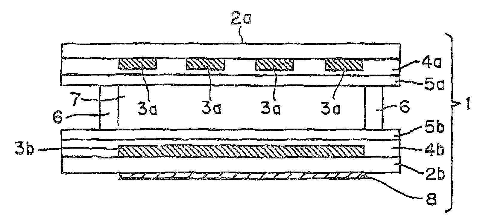
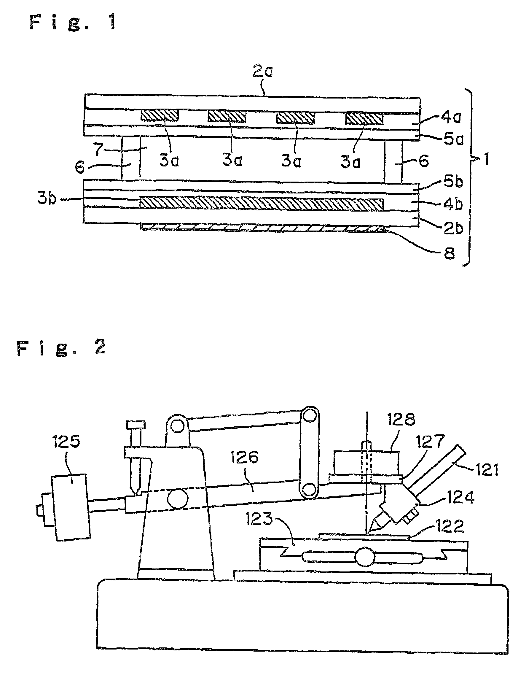
[0100]CL-LCD was prepared according to the manufacturing method described before. The line space was 10 μm and the number of stripe electrodes was 4. Each resin layer as a boundary layer was formed by using a solution of polyimide resin RN-1256 manufactured by Nissan Chemical Industries, Ltd. wherein the layer thickness was about 600 Å. In the measurement of the surface hardness of the resin layer according to the before-mentioned test method, it was found to be “B”. RN-1266 and RN-1286 which is used in Example 2 are a new material for an alignment layer, and the properties and so on are described in specifications provided by that company.
[0101]Then, a bipolar pulse of rectangular waveform (hereinbelow, referred to as a pulse A) having a pulse width of 900 ms and an effective value of 20 Vrms was applied to all pixels through electrodes of both substrate. Then, liquid crystal P became FC, and all the pixels exhibited a uniform black color. Then, a bipolar pulse of rectangular wavef...
example 2
[0104]A liquid crystal optical element was prepared by the same method as in Example 1 except that a solution of polyimide resin RN-1286 manufactured by Nissan Chemical Industries, Ltd. was used. The line space was 10 μm and the number of stripe electrodes was 160. The surface hardness of the resin layers was “3B”.
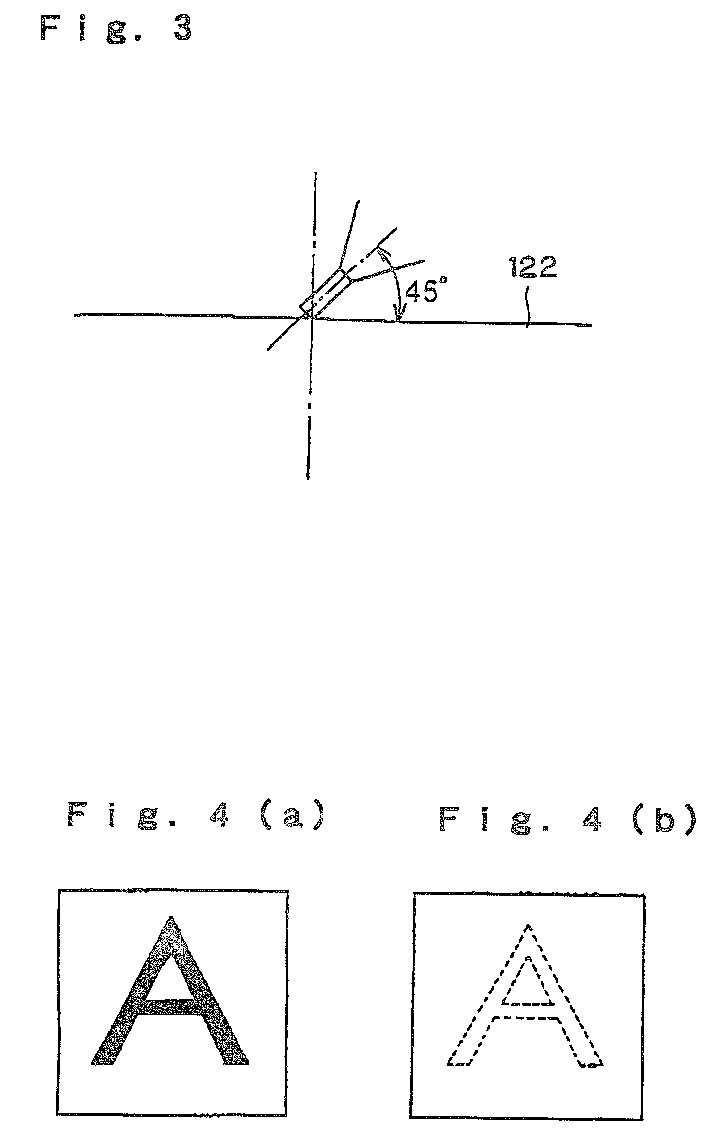
[0105]First, initialization was performed by applying a relatively high voltage to liquid crystal corresponding to each pixel to render the liquid crystal to be HO; by eliminating the voltage in such state, and applying further a voltage which rendered the liquid crystal to be FC. After the initialization, a-line-at-a-time driving was performed in one round with 160 row electrodes and 160 column electrodes to display a character of “A”, and then, the application of the voltage was stopped. As a result, a state that a character of “A” in a green color (PL) was displayed in a background of black color (FC), was provided. After the liquid crystal panel displaying a character ...
example 3
[0120]A liquid crystal panel was provided by the same method as Example 1 except that only a resin layer formed on a rear substrate was subjected to a rubbing treatment. As in Example 1, a black paint for delustering was applied on an outer side of the rear substrate. A drive pulse was applied across electrode leads (terminals) of both substrates. After a bipolar pulse of rectangular waveform having a pulse width of 20 msec and an effective value of 40V rms was applied, the drive pulse was cut off. Consequently, the liquid crystal layer that confronts to the entire display screen of the liquid crystal panel was instantly transformed into PL. Then, the liquid crystal layer was rendered into PL with normal reflection slightly added until about 30 sec were passed. After lapse of further several minutes, this state became stable at substantially the brightest level. There was no change even after the liquid crystal layer was left for five days.
[0121]Next, after a bipolar pulse of rectan...
PUM
| Property | Measurement | Unit |
|---|---|---|
| drive voltage | aaaaa | aaaaa |
| Young's modulus | aaaaa | aaaaa |
| temperature | aaaaa | aaaaa |
Abstract
Description
Claims
Application Information
 - R&D
- Intellectual Property
- Life Sciences
- Materials
- Tech Scout
- Unparalleled Data Quality
- Higher Quality Content
- 60% Fewer Hallucinations
Browse by: Latest US Patents, China's latest patents, Technical Efficacy Thesaurus, Application Domain, Technology Topic, Popular Technical Reports.
© 2025 PatSnap. All rights reserved.Legal|Privacy policy|Modern Slavery Act Transparency Statement|Sitemap|About US| Contact US: help@patsnap.com