Encapsulation for oled devices

a technology of oled devices and encapsulation, which is applied in the field of encapsulation of oled devices, can solve the problems of limiting the miniaturization of oled devices and inefficient use of chip area

Inactive Publication Date: 2007-08-14
OSRAM OPTO SEMICONDUCTORS GMBH +1
View PDF22 Cites 93 Cited by
  • Summary
  • Abstract
  • Description
  • Claims
  • Application Information

AI Technical Summary

Problems solved by technology

Such a large sealing width results in inefficient use of chip area, limiting miniaturization of OLED devices.

Method used


Image

  • Encapsulation for oled devices
  • Encapsulation for oled devices
  • Encapsulation for oled devices

Examples


example

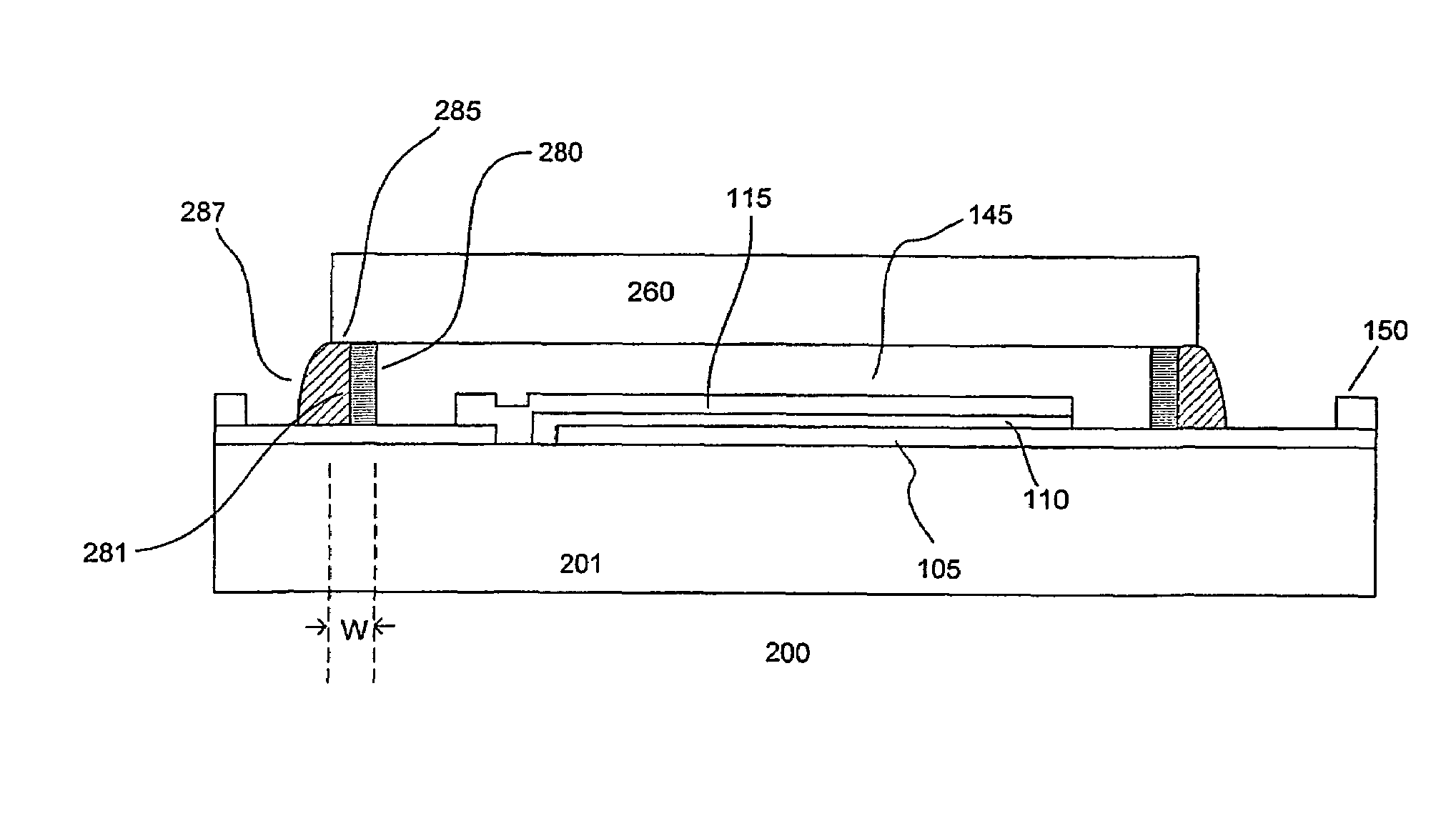
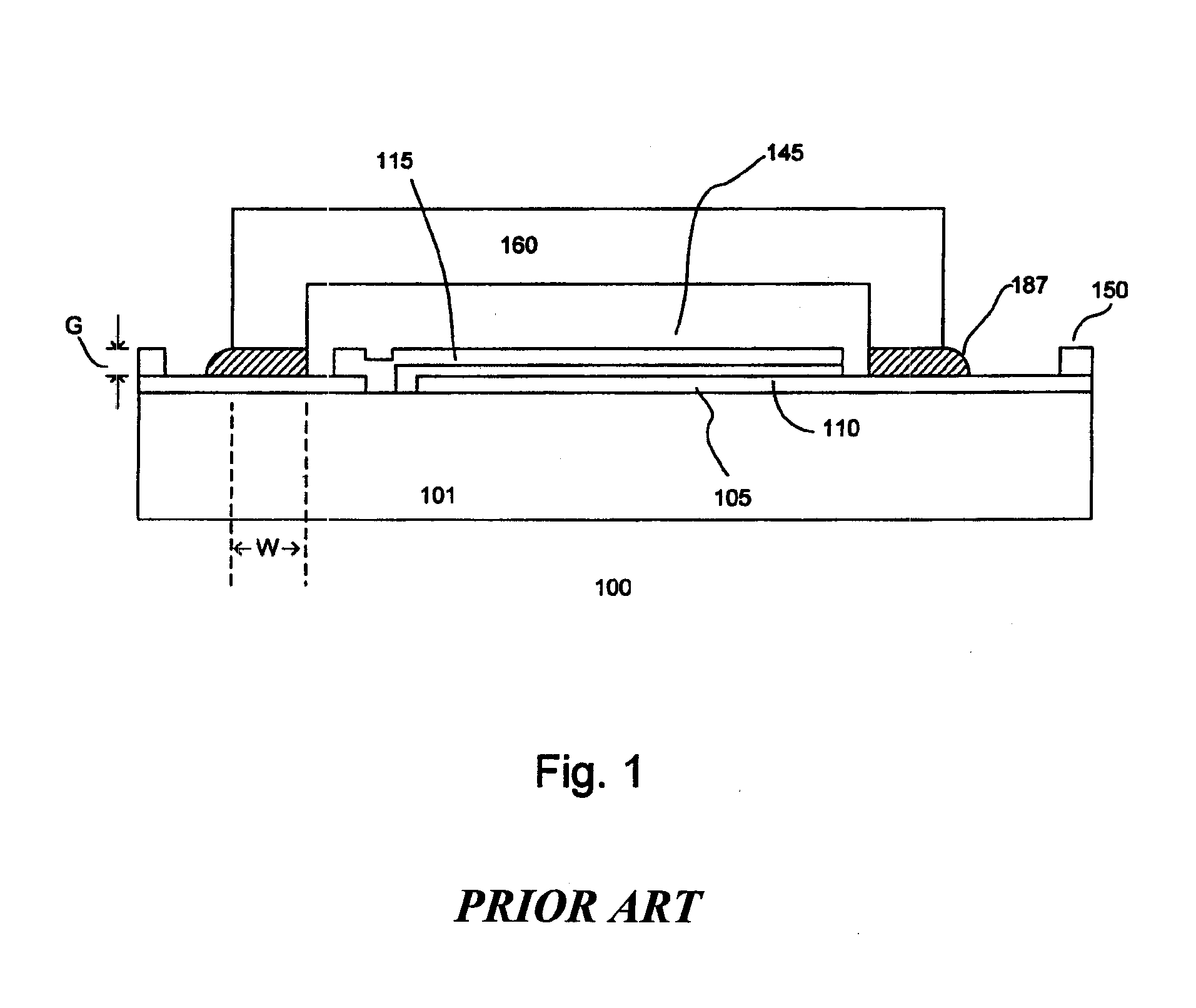
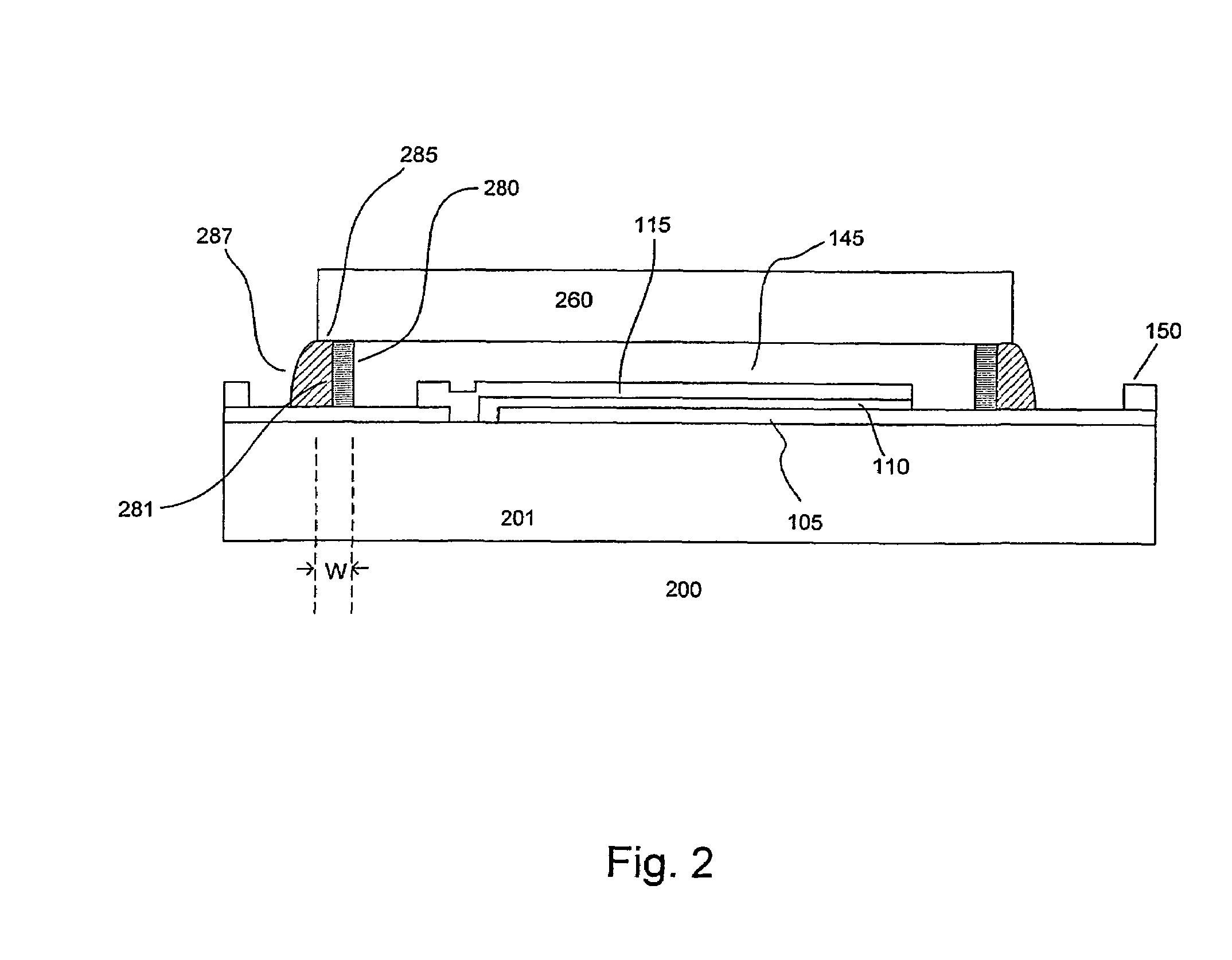
[0020]A 1 um thick layer of AZ 5214E photoresist was deposited onto a glass substrate. The glass substrate was about 22 mm2 and 100 um thick. A Karl Suess RC 8 spin-coater was used to deposit the photoresist (about 1000 rpm for about 20 seconds). Subsequently, the resist was baked at 90° C. for about 2 min to remove the solvent, resulting in a dry resist film of about 1.2 um thick. The dry resist film is selectively exposed with a 50 MJ / cm2 dose of UV light using a Karl Suess MJB 3 contact-exposing system.

[0021]After exposure, the resist was developed in AZ 726 alkaline developer for about 1 minute at room temperature. The exposed regions of the resist were dissolved, leaving the sealing dam on the substrate. The cap (substrate with the dam) was then mounted on a prepared substrate with OLED pixels. An adhesive was dispensed along the edges of the dam, encapsulating the device. In another experiment, prior to mounting the cap onto the prepared OLED substrate, it was baked at about 2...


PUM

PropertyMeasurementUnit
sealing widthaaaaaaaaaa
widthsaaaaaaaaaa
sealing widthaaaaaaaaaa

Abstract

An encapsulation for an organic light emitting diode (OLED) (201) device is disclosed. The encapsulation includes a sealing dam (280) surrounding the cell region of the OLED device to support a cap. The sealing dam provides a sealing region between the edge of the cap and dam in which an adhesive is applied to seal the OLED device. The use of the sealing dam advantageously enables devices to be formed with narrower sealing widths.

Description

FIELD OF THE INVENTION[0001]The present invention relates to organic light emitting diode (OLED) devices. More particularly, the invention relates to encapsulation of OLED devices.BACKGROUND OF THE INVENTION[0002]FIG. 1 shows a conventional OLED device 100. OLED devices can be used as displays in various consumer electronic products, including cellular phones, cellular smart phones, personal organizers, pagers, advertising panel, touch screen displays, teleconferencing equipment, multimedia equipment, virtual reality products, and display kiosks.[0003]The OLED device comprises a functional stack of one or more organic functional layers 110 between a transparent conductive layer 105 and a conductive layer 115. The functional stack is formed on a transparent substrate 101. The conductive layers can be patterned to form one or more cells or pixels on the substrate. Bond pads 150 are coupled to the cathodes and anodes to control the OLED pixels. In operation, charge carriers are injecte...

Claims


Application Information

Patent Timeline
Patent Type & Authority Patents(United States)
IPC IPC(8): B29C39/10G02F1/1339H05B33/04H01L51/50H01L51/52H05B33/10
CPCH01L51/5237H10K50/8428H10K50/8426
Inventor GUENTHER, EWALD KARL MICHAELAUCH, MARK DAI JOONG
Owner OSRAM OPTO SEMICONDUCTORS GMBH
Why Eureka
Try Eureka