Method for fabricating semiconductor device

a semiconductor and device technology, applied in the direction of electrical appliances, decorative surface effects, decorative arts, etc., can solve the problems of reducing the yield of the device, and achieve the effect of preventing the generation of undesired particles and simplifying the contact hole formation process

Inactive Publication Date: 2007-08-14
SK HYNIX INC
View PDF8 Cites 20 Cited by
  • Summary
  • Abstract
  • Description
  • Claims
  • Application Information

AI Technical Summary

Benefits of technology

[0009]It is, therefore, an object of the present invention to provide a method for forming a contact hole in a semiconductor device capable of simplifying the contact hole formation process and preventing a generation of undesired particles generally caused by an ex-situ etch process.

Problems solved by technology

As described above, if the conventional technology is applied, and the hard mask layer and the inter-layer insulation layer are etched separately in different chambers, undesired particles may be generated while moving the wafer into the different chambers during the device formation, resulting in a decreased device yield.

Method used


Image

  • Method for fabricating semiconductor device
  • Method for fabricating semiconductor device
  • Method for fabricating semiconductor device

Examples


Embodiment Construction

[0014]A method for fabricating a semiconductor device in accordance with specific embodiments of the present invention will be described in detail with reference to the accompanying drawings.

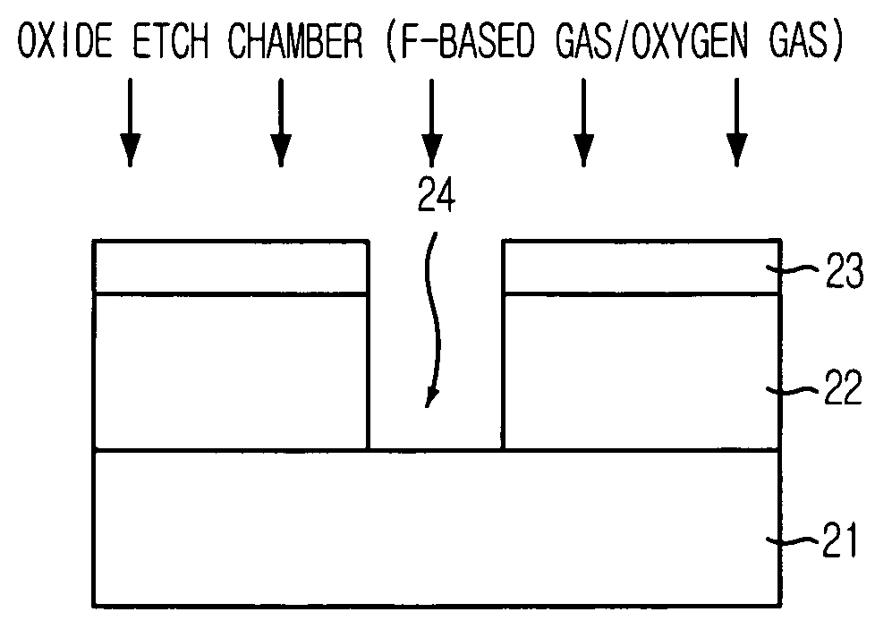
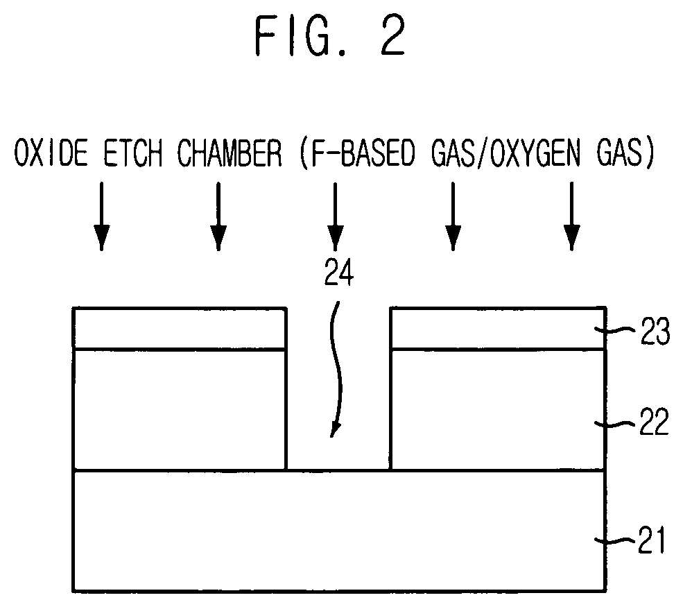
[0015]FIG. 2 is a cross-sectional view illustrating a method for fabricating a semiconductor device in accordance with a specific embodiment of the present invention.

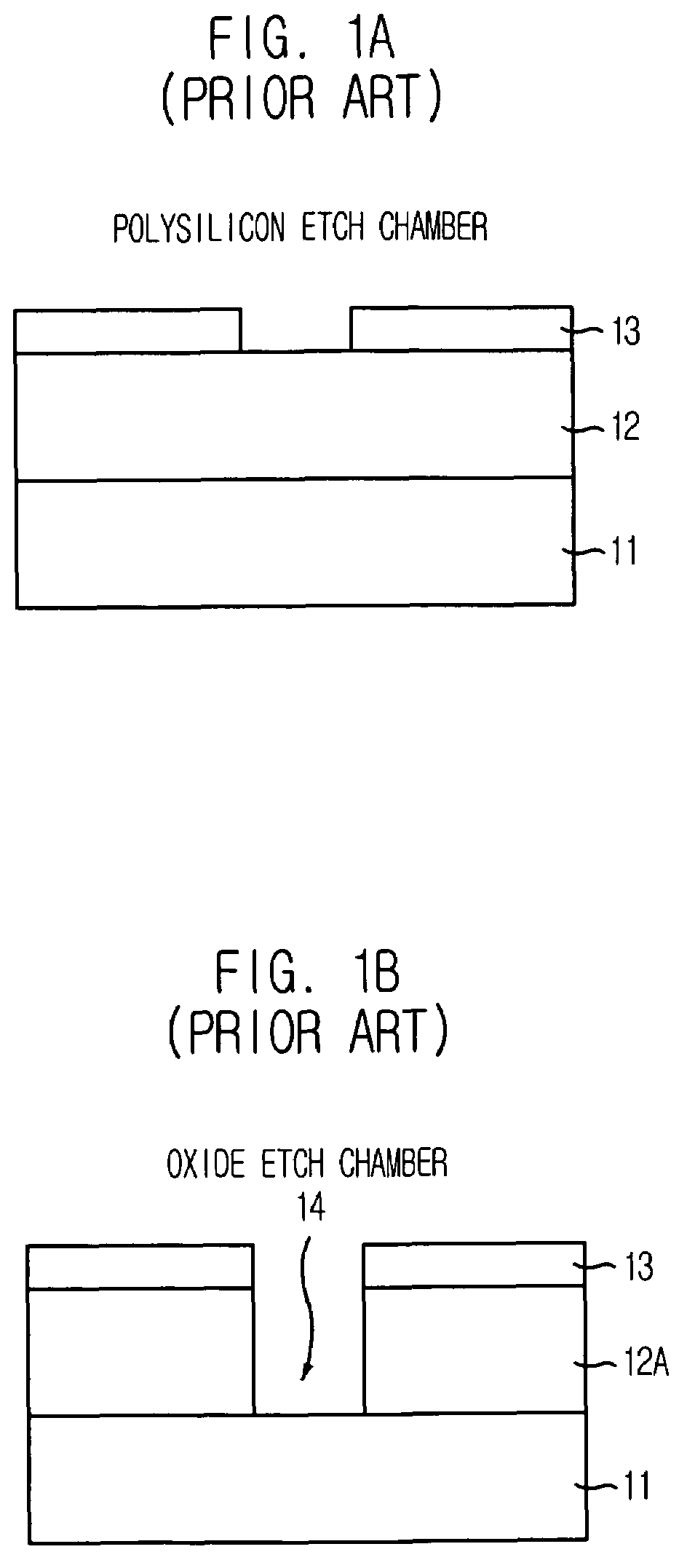
[0016]As shown in FIG. 2, an inter-layer insulation layer 22 is formed on a substrate 21. Then, a hard mask layer 23 is formed on the inter-layer insulation layer 22. Herein, the hard mask 23 includes polysilicon.

[0017]Subsequently, the wafer is loaded on an etch chamber for an oxide layer to form a contact hole, and an etch rate of the hard mask layer 23 in the above etch chamber should be maintained at approximately 1,000 Å per minute identical to that in another etch chamber for a polysilicon layer.

[0018]Therefore, the hard mask layer 23 is etched at a chamber pressure ranging from approximately 40 mtorr to approximately 100 mtor...


PUM

PropertyMeasurementUnit
poweraaaaaaaaaa
poweraaaaaaaaaa
poweraaaaaaaaaa

Abstract

A method for fabricating a semiconductor device is provided. The method includes: forming an inter-layer insulation layer on a substrate; forming a hard mask layer on the inter-layer insulation layer; etching the hard mask layer using a contact mask; and etching the inter-layer insulation layer using the hard mask layer as an etch barrier, thereby obtaining an opening wherein the etching of the hard mask layer and the etching of the inter-layer insulation layer are performed in one etch chamber.

Description

FIELD OF THE INVENTION [0001]The present invention relates to a method for fabricating a semiconductor device; and, more particularly, to a method for forming a contact hole in a semiconductor device.DESCRIPTION OF RELATED ARTS[0002]As the dynamic random access memory (DRAM) devices are shrinking, the depth of an inter-layer insulation layer of a metal contact under 100 nm technology is increasing above 30,000 Å, and such increment in depth of the inter-layer insulation layer is expected to grow even higher as the devices are becoming more shrunken.[0003]Especially for the devices of 90 nm level or under, the thickness of a photoresist is reduced, and a hard mask is formed with polysilicon as a solution to an increasing inter-layer insulation layer and a lack of photo-mask define ability. Hence, damage on a top contact portion caused by the decreased photoresist thickness is prevented by the polysilicon hard mask.[0004]FIGS. 1A to 1B are cross-sectional views illustrating a conventi...

Claims


Application Information

Patent Timeline
Patent Type & Authority Patents(United States)
IPC IPC(8): H01L21/302
CPCH01L21/31116H01L21/31144H01L21/32137H01L21/28
Inventor NAM, KI-WONCHEONG, JUNG-TAIK
Owner SK HYNIX INC
Why Eureka
Try Eureka