Semiconductor device having a guard ring

Active Publication Date: 2007-08-14
FUJITSU SEMICON LTD
View PDF3 Cites 31 Cited by
  • Summary
  • Abstract
  • Description
  • Claims
  • Application Information

AI Technical Summary

Benefits of technology

[0011]One object of the present invention is to provide a semiconductor device having a guard ring capable of blocking invasion of moisture or gas into the semiconductor device from outside effectively and with reliability.
[0012]Another object of the present invention is to provide a semiconductor device having a guard ring occupying a small area and yet capable of blocking invasion of moisture or gas into the semiconductor device effectively and with reliability.
[0020]According to the present invention, the region between the first and second guard rings is compartmented by the bridging conductor pattern extending continuously along the band form region between the first and second guard rings when viewed in the direction perpendicular to the substrate. Thus, even in the case moisture or gas has invaded to such a region, further penetration of the moisture or gas to the interior of the semiconductor device is blocked by the foregoing bridging conductor pattern. Thereby, the bridging conductor pattern functions as a compartment wall or a bulkhead. Thus, according to the present invention, by using the two guard rings, invasion of moisture or gas is blocked positively while suppressing the increase of area of the substrate surface occupied by the guard ring.
[0028]In the semiconductor device of the present invention, a very minute interconnection pattern is formed in the first multilayer interconnection structure of the lower layer by using a stringent design rule, and associated with this, the first and second guard rings are formed by a minute pattern with minute pitch or minute interval. Contrary to this, the design rule is less stringent in the second multilayer interconnection structure of the upper layer where a large via-diameter is used. Thereby, the third guard ring is formed by a wide conductor wall having a comparatively large width in correspondence to the via-diameter. In the present invention, the area of the substrate surface occupied by the guard ring is minimized by providing the first and second guard rings right underneath the third guard ring. Of course, the reliability of the guard ring, and thus the reliability of the semiconductor device, can be improved furthermore by forming a different bridging conductor pattern in the first multilayer interconnection structure so as to bridge the first and second guard rings.

Problems solved by technology

On the other hand, in recent semiconductor integrated circuits of high integration density, it is insufficient to use a single interconnection layer for wiring semiconductor devices of enormous numbers formed on the substrate, and thus, a multilayer interconnection structure in which a number of interconnection layers are stacked with intervening insulation films is used generally for providing the necessary interconnection.

Method used


Image

  • Semiconductor device having a guard ring
  • Semiconductor device having a guard ring
  • Semiconductor device having a guard ring

Examples


first embodiment

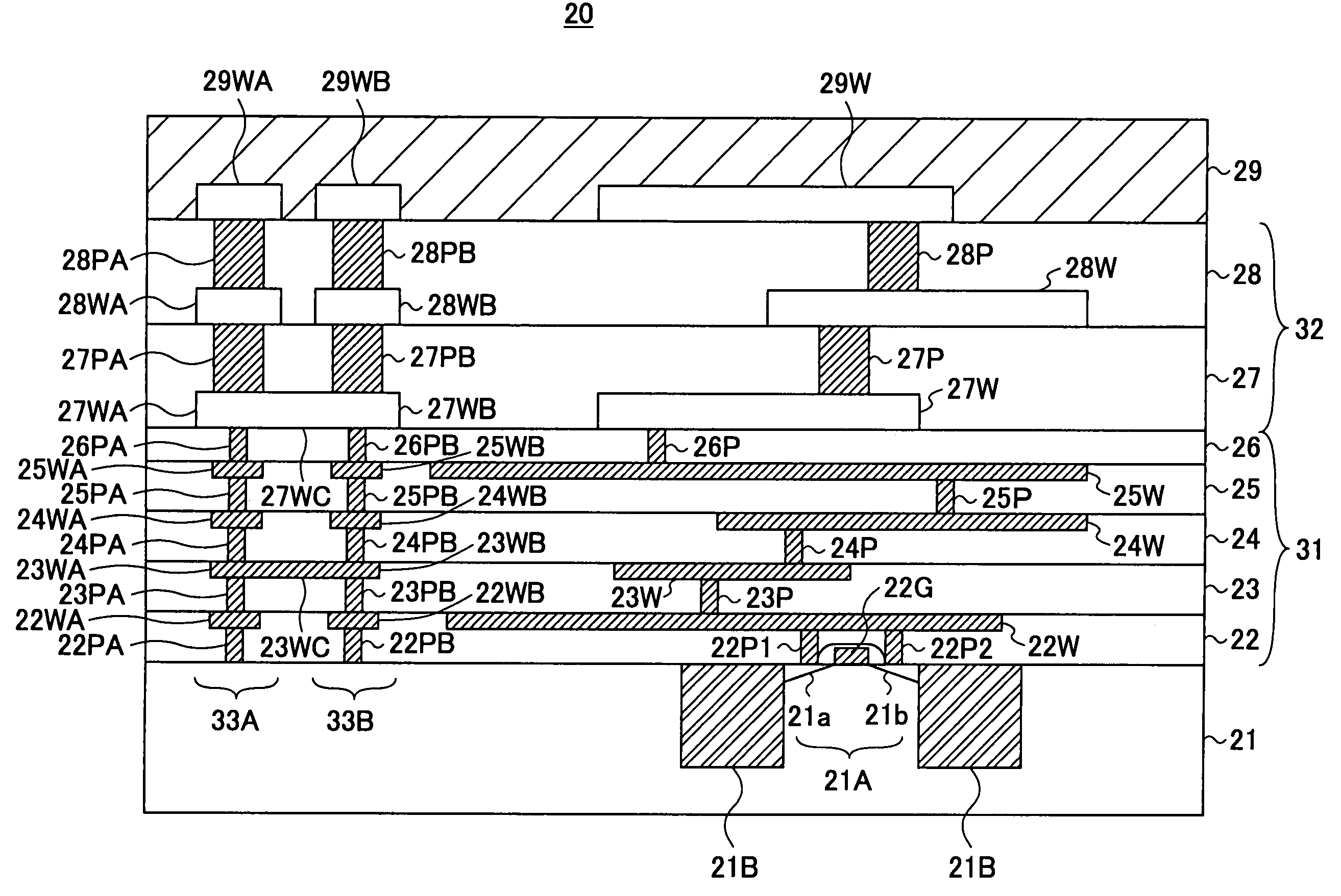
[0052]FIG. 3 shows the construction of a semiconductor integrated circuit 20 according to a first embodiment of the present invention.

[0053]Referring to FIG. 3, the semiconductor integrated circuit 20 is formed on a Si substrate 21 having a device region 21A defined by a device isolation structure 21B, and a MOS transistor including a gate electrode 22G and diffusion regions 21a and 21b is formed in the device region 21A such that the diffusion regions 21a and 21b are formed in the Si substrate 21 at both lateral sides of the gate electrode 22G. In FIG. 3, it should be noted that illustration of the gate insulation film is omitted. Further, similarly to a usual MOS transistor, the gate electrode 22G is provided with a pair of sidewall insulation films of SiO2 or SiON.

[0054]The gate electrode 22G is covered by an interlayer insulation film 22 formed on the substrate 21, wherein the interlayer insulation film 22 forms a part of the first multilayer interconnection structure 31 formed ...

second embodiment

[0085]FIG. 9 shows the construction of a semiconductor device 40 according to a second embodiment of the present invention, wherein those parts corresponding to the parts explained previously are designated by the same reference numerals and description thereof will be omitted.

[0086]Referring to FIG. 9, the interval between the guard ring 33A and the guard ring 33B on the substrate 21 is reduced in the present embodiment, and associated with this, there is formed, on the conductor pattern 27WC, a single guard ring 33C in the form of stacking of: a single conductor wall 27PC corresponding to the conductor plug 27P; a single conductor pattern 28WC corresponding to the interconnection layer 28W; a single conductor wall 28PC corresponding to the conductor plug 28P; and a single conductor pattern 29WC corresponding to the interconnection layer 29W.

[0087]As shown in FIG. 9, in the semiconductor device of the construction in which the multilayer interconnection structure 32 including there...


PUM


Abstract

A multilayer interconnection structure of a semiconductor device includes a first guard ring extending continuously along a periphery of a substrate and a second guard ring extending continuously in the multilayer interconnection structure along the periphery so as to be encircled by the first guard ring and so as to encircle an interconnection pattern inside the multilayer interconnection structure, wherein the first and second guard rings are connected with each other mechanically and continuously by a bridging conductor pattern extending continuously in a band form along a region including the first and second guard rings when viewed in the direction perpendicular to the substrate.

Description

CROSS-REFERENCE TO RELATED APPLICATION[0001]The present application is based on Japanese priority application No. 2003-088139 filed on Mar. 27, 2003, the entire contents of which are hereby incorporated by reference.BACKGROUND OF THE INVENTION[0002]The present invention generally relates to semiconductor devices and more particularly to a semiconductor device having a multilayer interconnection structure.[0003]Conventionally, increase of operational speed has been attempted in semiconductor devices by way of device miniaturization according to the scaling law. On the other hand, in recent semiconductor integrated circuits of high integration density, it is insufficient to use a single interconnection layer for wiring semiconductor devices of enormous numbers formed on the substrate, and thus, a multilayer interconnection structure in which a number of interconnection layers are stacked with intervening insulation films is used generally for providing the necessary interconnection.[0...

Claims


Application Information

Patent Timeline
Patent Type & Authority Patents(United States)
IPC IPC(8): H01L23/544H01L21/3205H01L23/52H01L23/00H01L23/58
CPCH01L23/564H01L23/585H01L2924/0002H01L2924/00
Inventor WAKAYAMA, SHIGETOSHIKAI, MUTSUAKIKATO, HIROYUKISUGA, MASATO
Owner FUJITSU SEMICON LTD
Why Eureka
Try Eureka