
Multi-stage charge pump voltage generator with protection of the devices of the charge pump

a charge pump and voltage generator technology, applied in the direction of electric variable regulation, power conversion systems, instruments, etc., can solve the problems of reducing the output voltage vsub>out to zero, affecting the correct operation of the powered electronic circuit, and the penalty of using high-voltage transistors for the charge pump circuit. , to achieve the effect of reducing the requirement of silicon area and efficient and effective approach

Active Publication Date: 2007-08-14
STMICROELECTRONICS SRL
View PDF6 Cites 29 Cited by
  • Summary
  • Abstract
  • Description
  • Claims
  • Application Information

AI Technical Summary

Benefits of technology

This approach effectively protects the charge pump transistors from abrupt voltage drops while minimizing silicon area requirements and maintaining efficient operation by allowing voltage to decrease gradually, reducing the risk of damage and optimizing capacitance design.

Problems solved by technology

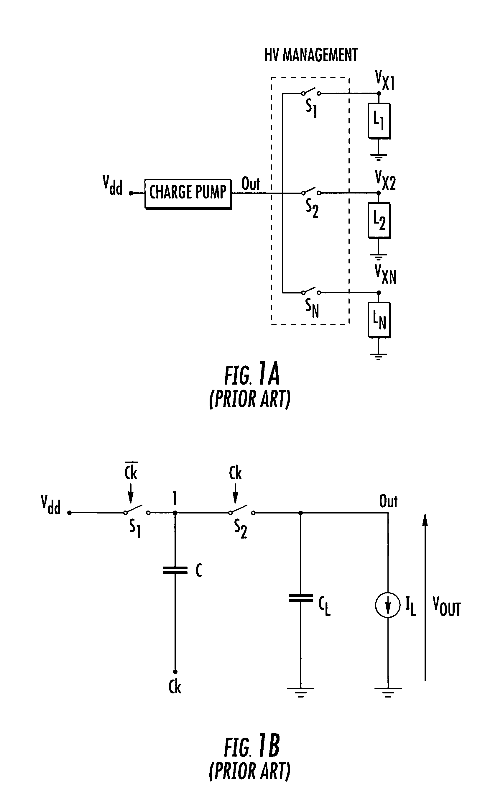
Keeping the output boosted voltage VOut of a charge pump substantially constant for ensuring the correct operation of the powered electronic circuits may be difficult in certain situations.
If for example the load capacitance is practically discharged when a certain load is switched to the output node of the powering boosted voltage generator, the charge pump circuit may be momentarily unable to provide the specified voltage, and the output voltage VOut may even drop to zero.
However, there is a penalty in using high-voltage transistors for the charge pump circuit because of the increased silicon area required.
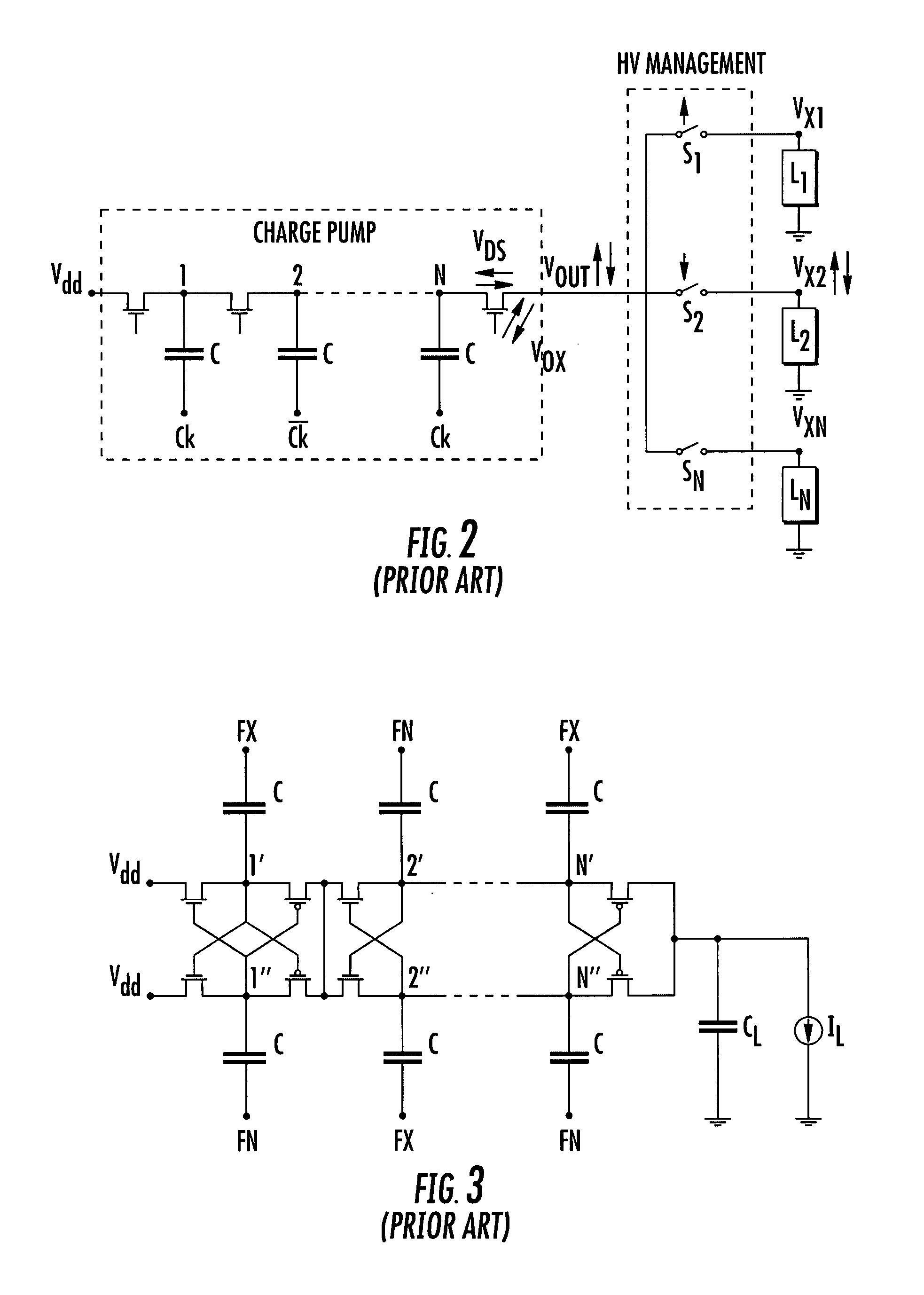
In this situation, the transistors of the last stage of the multistage charge pump are likely to be damaged through the breaking of their gate oxide if the applied voltage VOX becomes larger than the design supply voltage Vdd.
Moreover, because the channels of normal low-voltage transistors are relatively shorter than those of high-voltage transistors, if the drain-source voltage VDS exceeds the supply voltage Vdd, the channels are likely to be punched-through and the transistors damaged.
Unfortunately, a constant voltage VOutInt implies that the current IOut delivered by the charge pump be constant and this is a drawback both in transient as well as in steady state conditions.
If the voltage on the load is VXMax, then the voltage limiter does not introduce any loss of efficiency, while if it is smaller than VXMax, the voltage limiter causes inefficiency by not allowing the voltage VOutInt to become smaller than the voltage VXMax.
By summarizing, the drawback of using the voltage limiter is that of fixing the voltage VOutmim.
If VOutmin is smaller than VXMax the charge pump may be damaged.
The voltage VOutInt may undergo a large and abrupt reduction that could damage the transistors of the charge pump.
This is inconvenient.
Therefore, in a half-period of 25 ns of the clock, the voltage VOutInt would drop by about 25-50V, and this is very risky for the charge pump integrity.
Unfortunately, the required additional capacitor occupies a relatively large silicon area.

Method used


Image

  • Multi-stage charge pump voltage generator with protection of the devices of the charge pump
  • Multi-stage charge pump voltage generator with protection of the devices of the charge pump
  • Multi-stage charge pump voltage generator with protection of the devices of the charge pump

Examples


Embodiment Construction

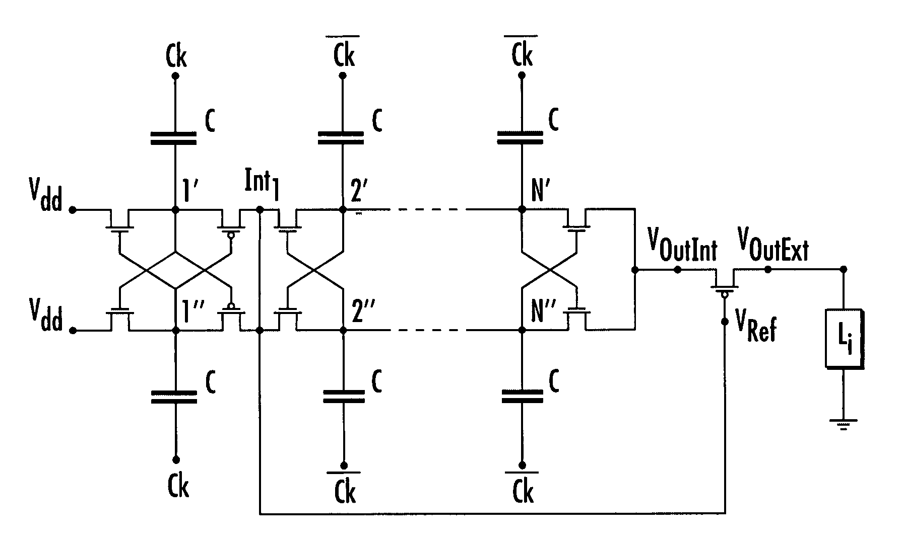
[0049]According to this invention, the output voltage VOutInt of the charge pump is effectively limited and forced to decrease gradually while using a circuit architecture with similar features to that of FIG. 7. According to this invention, the voltage VRef is not constant, as in the prior art, but is kept substantially constant only during the same half-period of the clock, especially during the half-period in which the voltage VOutExt drops abruptly, and varies during the other half-periods of the clock. The variations ΔVf of the voltage VOutInt are given by the following equation:

ΔVf=VOutInt−VOutmin=VOutInt−(VRef+VTh)  (11)

[0050]By connecting the control node of the added high voltage PMOS output transistor to an intermediate node Int of the charge pump, that is to the connection node of two stages of the multi-stage charge pump, as shown in FIG. 14, and in particular for a latch charge pump as shown in FIG. 15, after several clock periods, the voltage VRef follows the voltage V...


PUM


Abstract

Protecting the devices of a charge pump includes the connection of a high-voltage transistor between the output node of the charge pump and the load being supplied, and in controlling this transistor with a fraction of the output voltage of the charge pump. This control is accomplished by connecting the control node of the high-voltage transistor to a node of connection between two stages of the multi-stage charge pump onto which a fraction of the controlled output voltage of the multi-stage charge pump is produced. The high-voltage output transistor protects the low voltage devices of the multi-stage charge pump, by preventing the controlled output voltage from undergoing excessively abrupt variations, that could damage the transistors of the last stage of the charge pump.

Description

FIELD OF THE INVENTION[0001]The present invention relates to boosted voltage generators and more particularly to a multi-stage charge pump having a protection circuit for protecting the devices of the last stage of the multi-stage charge pump.BACKGROUND OF THE INVENTION[0002]Charge pump voltage generators are widely used for powering certain electronic circuits at a specified boosted voltage VOut (higher than the supply voltage) that must remain substantially constant notwithstanding variations of the current absorbed by the load currently connected to the output of the boosted voltage generator. Keeping the output boosted voltage VOut of a charge pump substantially constant for ensuring the correct operation of the powered electronic circuits may be difficult in certain situations.[0003]As depicted in FIG. 1A, in a nonvolatile memory device, the output node of the boosted voltage generator may be connected through an array of switches Si (i=1 . . . N) HV MANAGEMENT to respective lo...

Claims


Application Information

Patent Timeline
Patent Type & Authority Patents(United States)
IPC IPC(8): G05F1/10
CPCH02M3/073H02M1/32
Inventor UCCIARDELLO, CARMELODI MAURO, ROSAPAPPALARDO, DOMENICOSORRENTINO, FRANCESCOMAGANUCO, GIUSEPPEPALUMBO, GAETANO
Owner STMICROELECTRONICS SRL
Learn More