Method for the hermetic encapsulation of a component

a technology of component and hermetic encapsulation, which is applied in the direction of semiconductor devices, semiconductor/solid-state device details, electrical devices, etc., can solve problems such as component corrosion, and achieve the effect of simple implementation

Inactive Publication Date: 2007-08-21
SNAPTRACK
View PDF18 Cites 76 Cited by
  • Summary
  • Abstract
  • Description
  • Claims
  • Application Information

AI Technical Summary

Benefits of technology

[0004]It is therefore the object of the invention to specify a method for hermetic encapsulation of an electrical component which is simple to implement and prevents the disadvantages cited above.
[0006]In contrast to the prior art, the second metal layer is not applied by means of a galvanic process in which water as solvent penetrates into the component and can cause a corrosion of the component. Furthermore, the second metal layer is not applied on all regions on which the first continuous metal layer is present, but rather only on those regions of the first metal layer that cover the insulating material. This has the advantage that, in the inventive method, the consumption of the metal can be significantly reduced for the second metal layer.
[0007]A whole series of processes are considered for a solvent-free process in the method step B) to apply the second hermetically sealing metal layer. Thus, for example, it is possible to melt a metal foil onto the first metal layer. Before the application, this metal foil is advantageously adapted (stamped) to the contours of the first metal layer, such that it attaches to the first metal layer with a positive fit. This has the advantage that, upon melting of this metal foil on the first metal layer, the second metal layer is generated with homogenous layer thickness, such that it particularly tightly seals the component.
[0011]In another embodiment of the inventive method, in the method step B) the material is, for example, applied in the form of a plastic film, such that the plastic film covers the back side of the chip and simultaneously the edges of the film overlap the chip. The film is subsequently sealed with the substrate in the entire edge region around the chip. The first metal layer is then applied onto this plastic film in the further method step C). This variant of the inventive method has the advantage that the method steps B) (application of the plastic film) and the method step C) (application of the first continuous metal layer) can be particularly well optimized independent of one another. In cooperation with the last method step D), a particularly secure hermetic encapsulation of the electrical component is thus possible via the application of the second metal layer. In this variant of the inventive method, the second hermetically sealing metal layer is advantageously applied over the entire first continuous metal layer. It is thereby particularly advantageously ensured that, in components encapsulated according to this variant, no moisture can penetrate through both metal layers into the plastic film, and thus also into the component.
[0012]In a further variant of the inventive method, the metals for the first and second metal layer and the process conditions for the application of the second metal layer in the method step D) are selected such that, during the application of the second metal layer, a metal alloy with a melting point of more than 260° C. is formed at the boundary area between the two metal layers. This has the advantage that the metal alloy does not melt, and therefore is also not permeable or loses rigidity, upon soldering of the inventively encapsulated component, which normally ensues at temperatures below 260° C. Such encapsulated component can thus be soldered without large problems as SMD components by means of standard soldering methods.
[0013]As a first metal layer, a titanium-copper layer is advantageously applied in which a thicker copper layer is applied as a bonding agent to a very thin titanium layer. As a second metal layer, tin or eutectic tin alloys, for example, tin-silver, tin-copper or tin-silver copper alloys or a mix of the cited metals, are advantageously applied. This has the advantage that the cited metals or, respectively, metal alloys are very inexpensive for the first and second metal layer, but at the same time a non-eutectic tin-copper alloy with a melting point of greater than 260° C. is formed at the boundary area between the first metal layer and the second metal layer upon application of the second metal layer. By means of this variant of the inventive method, it is thus particularly advantageously possible to generate, by means of inexpensive output materials for both of the metal layers, an alloy with a particularly high melting point that can not be melted during standard soldering methods at standard temperature. The materials cited above for the second metal layer thereby exhibit melting points between approximately 217° C. and 232° C. before the alloy formation.

Problems solved by technology

In contrast to the prior art, the second metal layer is not applied by means of a galvanic process in which water as solvent penetrates into the component and can cause a corrosion of the component.

Method used


Image

  • Method for the hermetic encapsulation of a component
  • Method for the hermetic encapsulation of a component
  • Method for the hermetic encapsulation of a component

Examples


Embodiment Construction

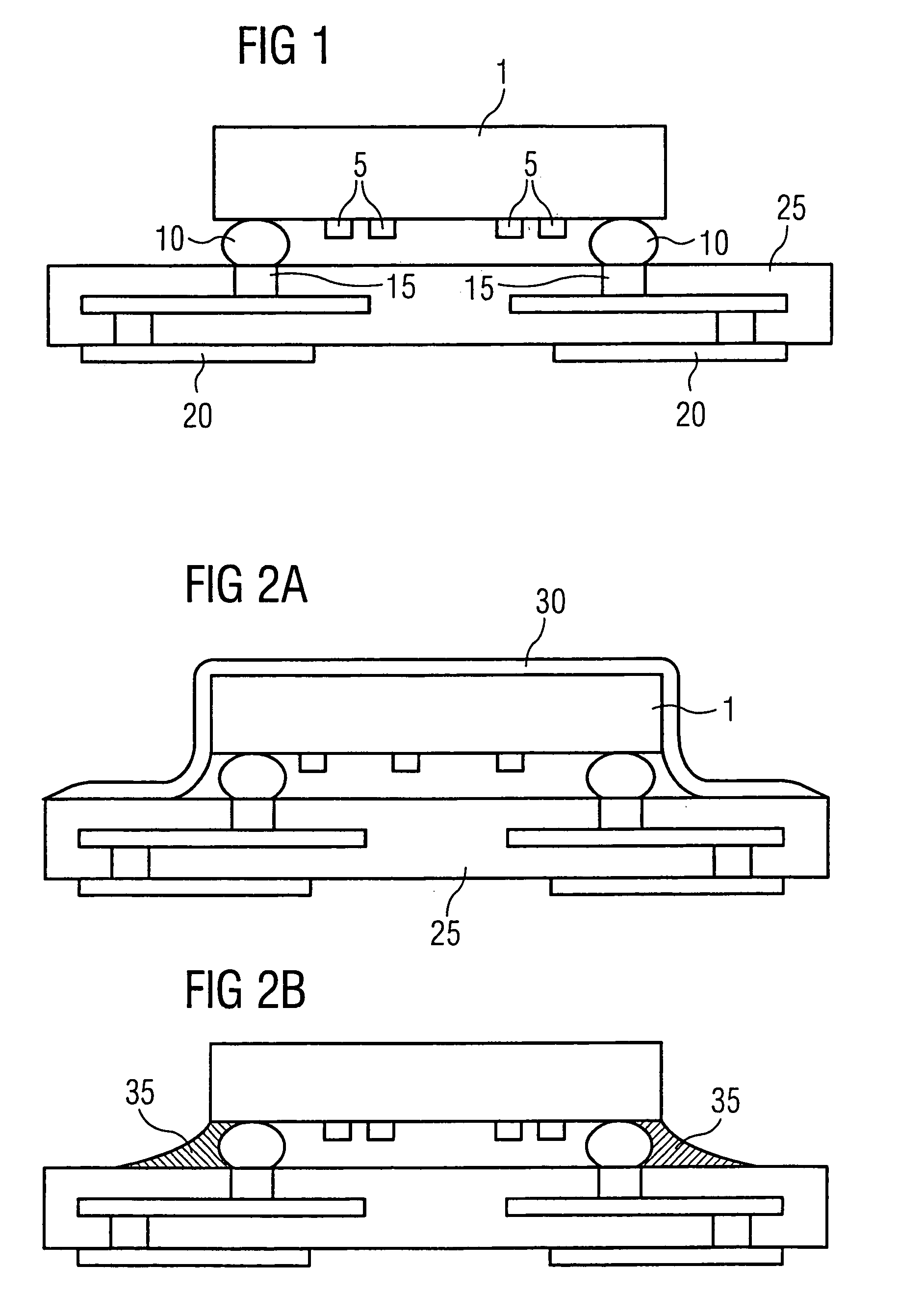
[0023]FIG. 1 shows an electrical component after the method step A). It is visible that a chip 1 is attached and contacted on a substrate 25 such that the component structures 5 located on the chip surface face the substrate 25. Solder balls 10 (bumps) thereby affix the component at a slight distance from the substrate and simultaneously electrically-conductively connect the connection areas 20 located on the substrate 25 with the component. A feedthrough 15 thereby provides for electrical contact between the connection areas 20 and the bumps 10.

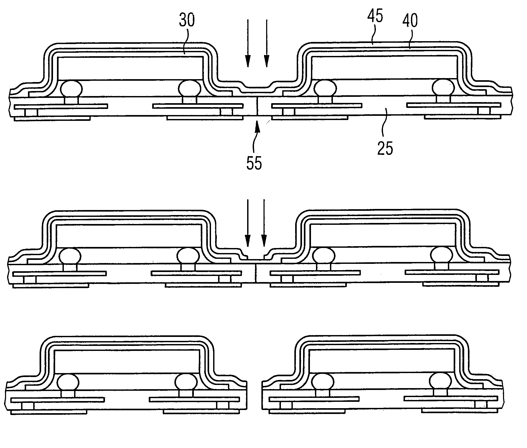
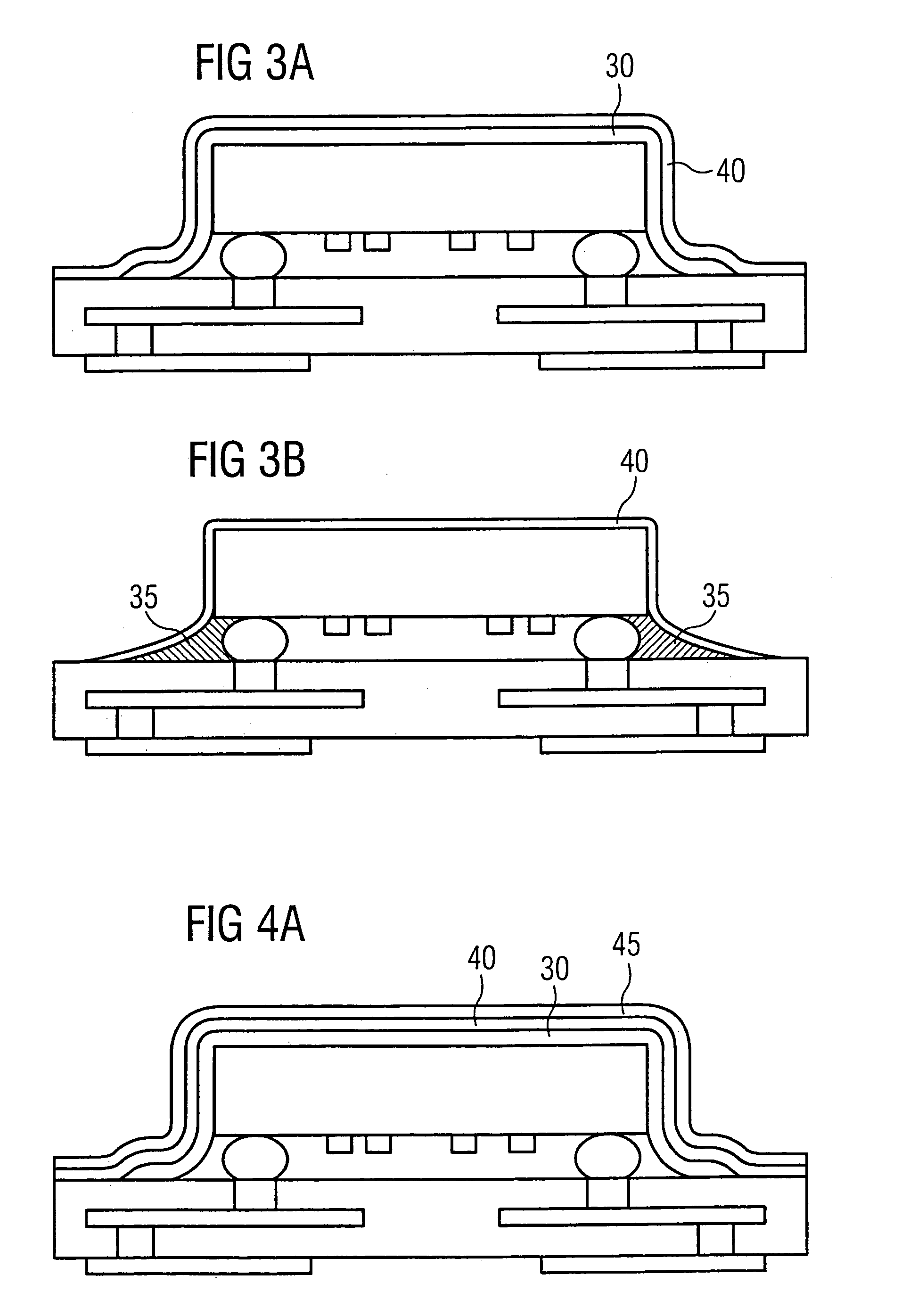
[0024]FIG. 2A shows a variant of the method steps B) of the inventive method. A plastic film 30 is continuously applied over the back side of the chip 1 and the regions of the substrate 25 abutting the chip, and has subsequently been sealed with the substrate in the entire edge region of the chip. An embodiment alternative to FIG. 2A is visible in FIG. 2B. The space between lower edge of the chip 1 and the regions of the substrate abutting t...


PUM

PropertyMeasurementUnit
melting pointaaaaaaaaaa
temperatureaaaaaaaaaa
temperaturesaaaaaaaaaa

Abstract

For hermetic encapsulation of a component, which includes a chip with component structures applied on a substrate in a flip-chip construction, a material is applied onto the lower edge of the chip and regions of the substrate abutting the chip, and then a first continuous metal layer is applied on the back side of the chip and on the material, as well as on edge regions of the substrate abutting the material. For hermetic encapsulation, a second sealing metal layer is subsequently applied by a solvent-free process at least on those regions of the first metal layer that cover the material.

Description

BACKGROUND OF THE INVENTION[0001]A method for hermetic encapsulation of a component is, for example, known from WO 99 / 43084. There components, in particular surface wave components, are applied in a flip-chip technique to a substrate provided with solderable connection areas. The component, which is fashioned on the chip, is thereby soldered to the substrate over bumps (solder balls) at a slight distance from the substrate, such that the component structures located on the chip face the substrate. For hermetic encapsulation of the components located on the substrate, said components are ultimately covered from the back with a metal foil or a metal-coated plastic film (first metal layer) on the substrate and glued or laminated. The foil thereby seals tight with the substrate between the components, such that an encapsulation is created for the component structures.[0002]After the application of the electrical component on the substrate, the lower edge of the chip and regions of the s...

Claims


Application Information

Patent Timeline
Patent Type & Authority Patents(United States)
IPC IPC(8): H01L21/50H01L21/44H01L21/48H01L23/552H01L23/04H01L21/56H03H9/10H03H9/25
CPCH01L21/561H01L24/97H03H9/1078H01L2224/97H01L2924/01004H01L2924/01029H01L2924/01033H01L2924/01047H01L2924/01052H01L2924/01078H01L2924/01079H01L2924/01082H01L2924/01322H01L2924/15174H01L2224/81H01L2224/16225H01L2224/32225H01L2224/73204H01L2924/01005H01L2924/01006H01L2924/01068H01L2924/00H01L2924/12042
Inventor STELZL, ALOISKRUEGER, HANSCHRISTL, ERNST
Owner SNAPTRACK
Why Eureka
Try Eureka