Thin film device supply body, method of fabricating thin film device, method of transfer, method of fabricating semiconductor device, and electronic equipment

a technology of thin film devices and supply bodies, applied in the direction of semiconductor devices, basic electric elements, electrical equipment, etc., can solve the problems of difficult handling of each thin film device individually and conducting inspection or mounting processes promptly, and achieves easy peeled and transferred, easy handling in fabrication and shipment, and flexibility.

Active Publication Date: 2007-08-28
SAMSUNG ELECTRONICS CO LTD
View PDF23 Cites 46 Cited by
  • Summary
  • Abstract
  • Description
  • Claims
  • Application Information

AI Technical Summary

Problems solved by technology

However, the flexible thin film device fabricated by using conventional transfer techniques as mentioned above has a disadvantage in that handling is difficult due to an unstable shape while the flexible thin film device is lightweight and flexible.
That is, the same method for handling conventional glasses or silicon wafers easily causes mistakes of dropping, etc., in holding or transferring a substrate due to the pliability of the substrates.
Particularly, in a case where a thin film device is fabricated in large quantity that is divided into a comparatively small area of approximately from several square millimeters to several square centimeters, it is very difficult to handle each thin film device individually and to conduct inspection or mounting processes promptly.
In addition, transferring a layer to be transferred to a transfer body that is soft (like film) makes a peeling operation difficult.
Even if a transfer body that is hard is used as a temporary transfer substrate (the first transfer body), a problem still arises in which the first transfer body is hardly detached from the second transfer body (to which a layer to be transferred is bonded if a substrate to be transferred (the second transfer body) to which the transfer is finally conducted) is composed of a material that has pliability or flexibility such as film, etc.
Also, even if the first transfer body is composed of a material that can be removed by etching etc., for example, a problem arises in which material selection is complicated.

Method used


Image

  • Thin film device supply body, method of fabricating thin film device, method of transfer, method of fabricating semiconductor device, and electronic equipment
  • Thin film device supply body, method of fabricating thin film device, method of transfer, method of fabricating semiconductor device, and electronic equipment
  • Thin film device supply body, method of fabricating thin film device, method of transfer, method of fabricating semiconductor device, and electronic equipment

Examples


first embodiment

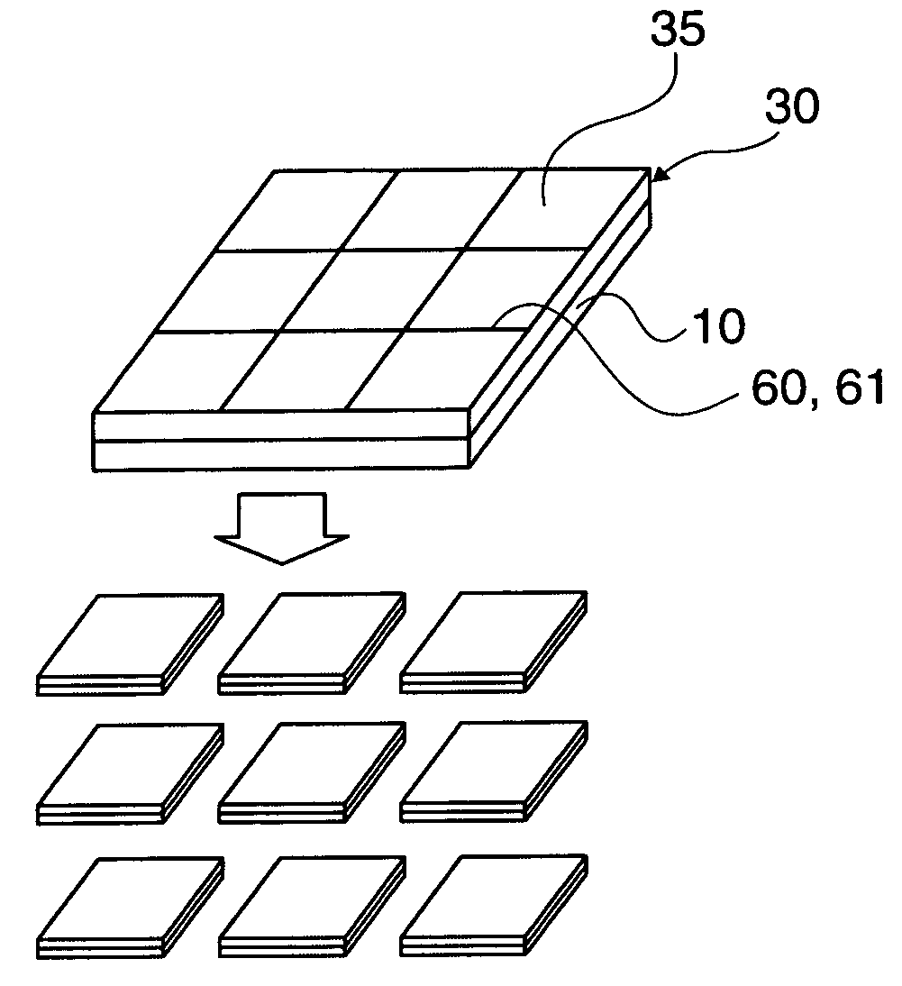
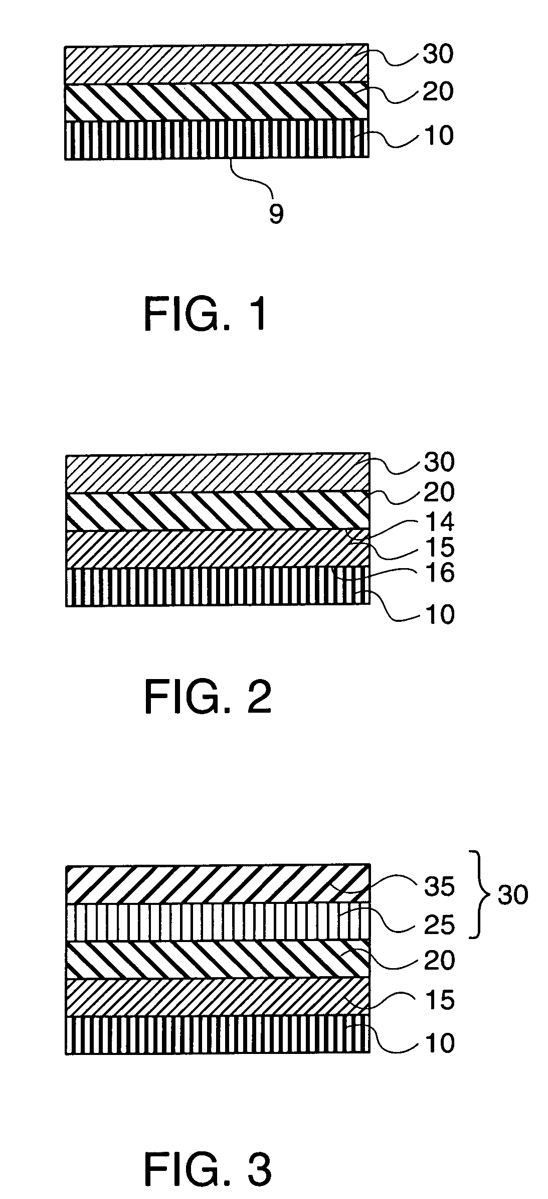
[0053]FIG. 1 shows a thin film device supply body according to a first embodiment of the present invention. As shown in the figure, in the thin film device supply body, a thin film device 30 is formed on one surface (the upper surface) of a supporting substrate 10 with a temporary fixing adhesive layer 20.

[0054]The supporting substrate 10 stably supports the thin film device. Glass such as soda glass, heat resistant glass such as Corning 7059 (product name), Nippon Electric Glass OA-2 (product name), etc., or silicon wafer etc., can be used for the supporting substrate 10 in addition to quartz glass. These substrates are hard and have excellent characteristics in shape stability.

[0055]The supporting substrate 10 is preferably a substrate that has light transparency in order to supply light energy (or heat) to the temporary fixing adhesive layer 20 from a back face 9 of the supporting substrate 10.

[0056]The temporary fixing adhesive layer 20 preferably has a characteristic in that ad...

second embodiment

[0062]FIG. 2 shows a second embodiment of the present invention. In the figure, portions corresponding to those in FIG. 1 are given the same numerals and the explanation thereof is omitted.

[0063]In the thin film device supply body of the embodiment, the supporting substrate 10 includes a first peeling layer 15. The thin film device 30 is formed on the upper surface of the peeling layer 15 (the surface that is not touched to the supporting substrate 10) with the temporary fixing adhesive layer 20. That is, the peeling layer 15 and the temporary fixing adhesive layer 20 are sandwiched between the supporting substrate 10 and the thin film device 30. As described later, an amorphous silicon layer, etc., can be used as the peeling layer 15. In the peeling layer 15, for example, the interatomic or intermolecular bonding force is lost by applying energy with laser light. As a result, peeling (destruction) occurs in the peeling layer 15, at an interface 16 of the peeling layer 15 and the su...

third embodiment

[0065]FIG. 3 shows a third embodiment of the present invention. In the figure, portions corresponding to those in FIG. 1 are given the same numerals and the explanation thereof is omitted.

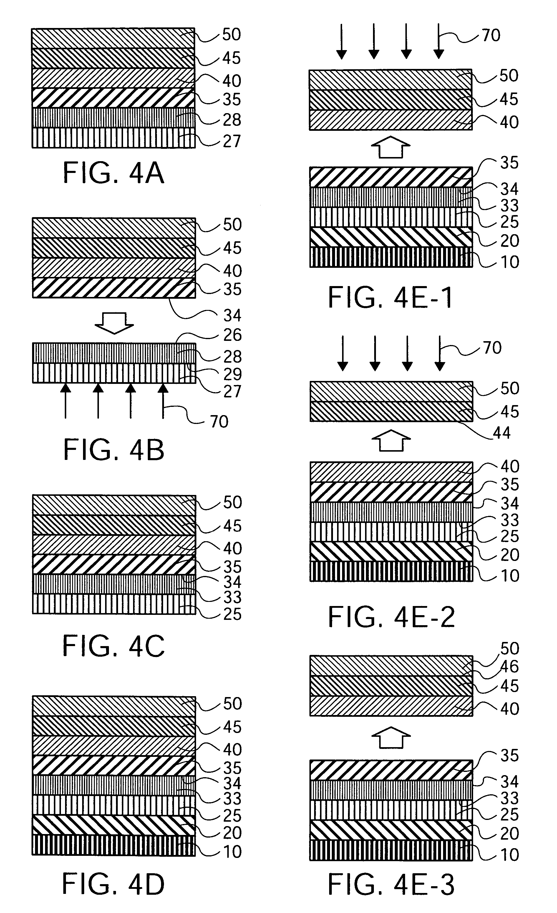
[0066]In the thin film device supply body of the embodiment, the thin film device 30 is bonded to the supporting substrate with the peeling layer 15 and the temporary fixing adhesive layer 20. The thin film device 30 is composed of a flexible substrate 25, a thin film element layer 35 formed on the flexible substrate 25, and the like. The thin film device 30 is bonded to the flexible substrate 25 with an adhesive layer that is not shown in the figure and will be described later as a permanent adhesive layer 33 in FIG. 4. That is, the thin film device supply body is formed as the stacked structure of the supporting substrate 10, the peeling layer 15, the temporary fixing adhesive layer 20, the flexible substrate 25, the permanent adhesive layer 33, and the thin film element layer 35.

[0067]The flexib...


PUM


Abstract

A technique is described in which a layer to be transferred is easily peeled and transferred to a transferred body that is pliable or flexible. Also, a method of fabricating a semiconductor device using these peeling and transfer techniques, and electronic equipment fabricated with the semiconductor device is described. A transfer method in which a layer to be transferred formed on a substrate is transferred to a transfer body that is pliable or flexible includes the first step of forming a layer to be transferred on a substrate; the second step of bonding the layer to be transferred formed on the substrate to a transfer body that is pliable or flexible fixed on a fixture; and the third step of peeling the layer to be transferred from the substrate and transferring the layer to be transferred to the transfer body.

Description

RELATED APPLICATION INFORMATION[0001]This application is related to and claims priority to Japanese Application No. JP2004-067556, filed Mar. 10, 2004, whose contents are expressly incorporated herein by reference.TECHNICAL FIELD[0002]Aspects of the present invention relate to a transfer technique of a thin film element, and in detail to a transfer method by which peeling and transferring can readily be conducted even though a transfer body is pliable or flexible, a method of fabricating a semiconductor device, and electronic equipment.BACKGROUND[0003]Recently, with respect to fabrication of thin film devices provided with thin film transistors (TFTs), thin film diodes (TFDs), etc., techniques have been examined in which a thin film device that is lightweight, excellent in shock resistance and is flexible is fabricated by transferring a thin film element, for example, to a flexible substrate that has flexibility from an original fabrication substrate, in which the thin film element ...

Claims


Application Information

Patent Timeline
Patent Type & Authority Patents(United States)
IPC IPC(8): H01L21/336H01L21/8234H01L21/68H01L51/00H01L51/40
CPCH01L21/6835H01L21/76251H01L27/1214H01L2924/19041H01L51/0013H01L2221/68359H01L2221/68363H01L27/1266H10K71/18H10K71/80
Inventor KODAIRA, TAIMEIUTSUNOMIYA, SUMIO
Owner SAMSUNG ELECTRONICS CO LTD
Why Eureka
Try Eureka