

Manufacturing process of a semiconductor non-volatile memory cell
a manufacturing process and non-volatile technology, applied in the direction of basic electric elements, electrical equipment, semiconductor devices, etc., to achieve the effect of improving electric properties and facilitating process integration
- Summary
- Abstract
- Description
- Claims
- Application Information
AI Technical Summary
Benefits of technology
Problems solved by technology
Method used
Image

Examples
second embodiment
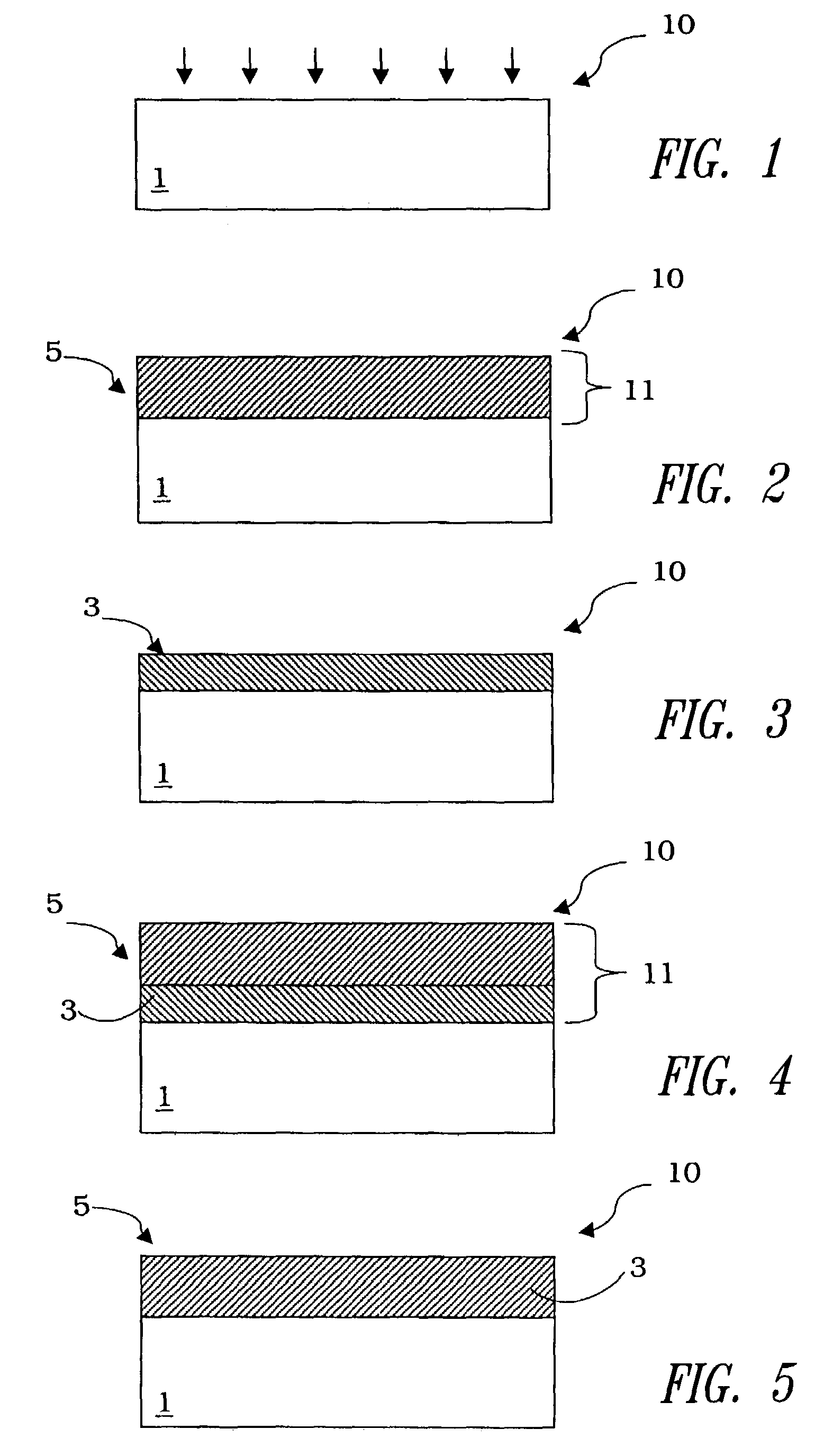
[0039]A second embodiment according to the invention is shown in FIGS. 3 and 4.
first embodiment
[0040]Elements having the same construction and function as in FIG. 2 are denoted for clarity with the same reference numerals, and are not described further.
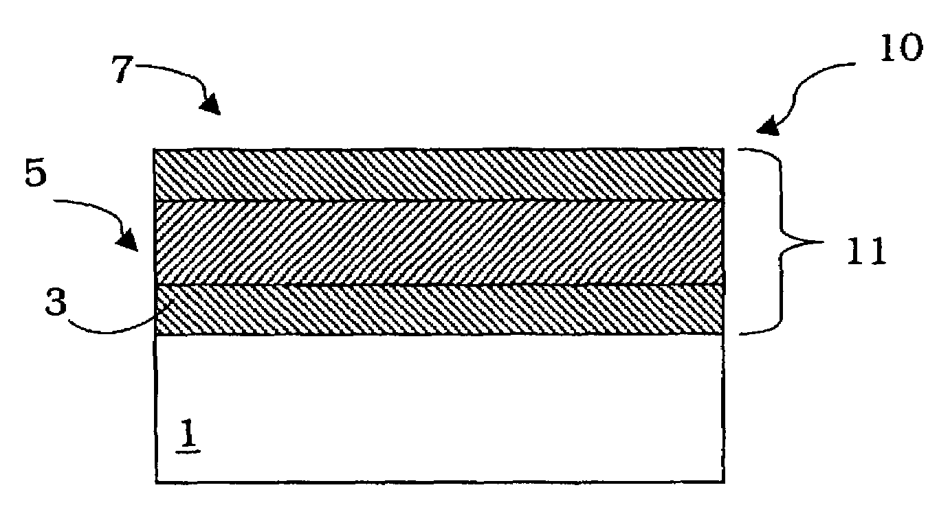
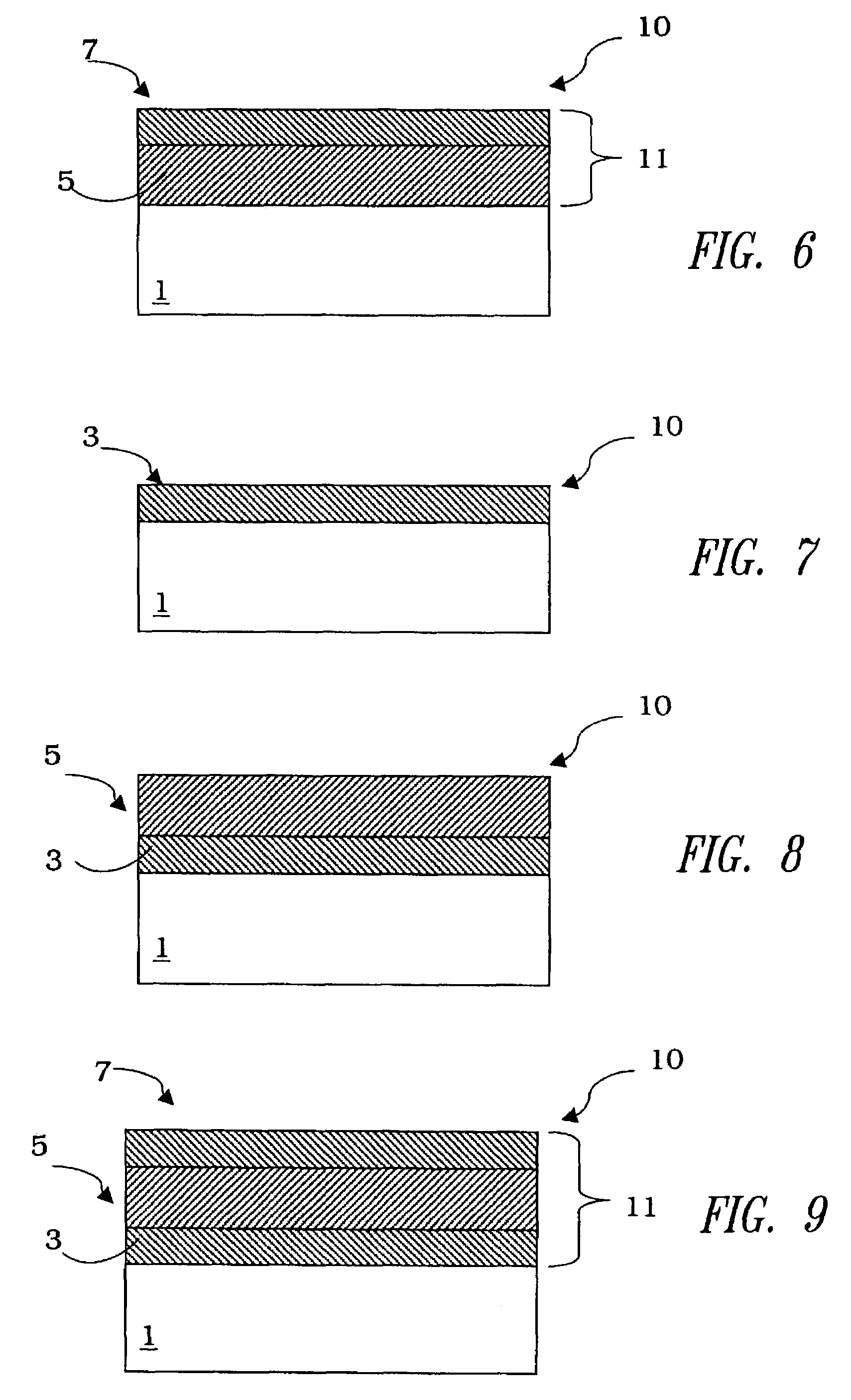
[0041]In particular, in the second embodiment of the invention, the interpoly dielectric layer 11 comprises the dielectric layer 5 with a high dielectric constant and another dielectric layer 3, known as the bottom dielectric. The bottom dielectric layer 3 is to isolate the dielectric layer 5 having a high dielectric constant from the floating gate region 1.
[0042]Advantageously, the bottom dielectric layer 3 is silicon dioxide, or a layer of a dielectric material whose dielectric constant is comprised in the range of 3.9 to 10.
[0043]The thickness of the bottom dielectric layer 3 can be selected in the range of 0.5 to 6.0 nm, it being understood that such values are measured in terms of EOT (Equivalent Oxide Thickness).
[0044]In one embodiment, the bottom dielectric layer 3 is an alumina layer, Al2O3, whose dielectric constant is...
third embodiment
[0046]A third embodiment according to the invention is shown in FIGS. 5 and 6.
[0047]Elements having the same construction and function as in the embodiment of FIG. 2 are denoted for clarity with the same reference numerals, and no further described.
[0048]In particular, in the third embodiment of the invention, the interpoly dielectric layer 11 comprises the dielectric layer 5 with a high dielectric constant and an additional dielectric layer 7, known as the top dielectric.
[0049]In particular, the dielectric layer 5 with a high dielectric constant is formed over the polysilicon layer 1, and the top dielectric layer 7 is then formed over the dielectric layer 5 having a high dielectric constant. The top dielectric layer 7 may be a silicon dioxide layer or a layer of a dielectric material whose dielectric constant lies in the range of 3.9 to 10.
[0050]The thickness of the top dielectric layer 7 can be selected in the range of 0.5 to 10 nm, it being understood that such values are measure...
PUM
 Abstract
Description
Claims
Application Information