Making method for MOS (Metal Oxide Semiconductor) transistor

A technology of MOS transistors and manufacturing methods, which is applied in the field of MOS transistor manufacturing, can solve problems such as performance deviations of MOS transistor devices, and achieve the effects of improving consistency, facilitating process integration, and reducing thickness deviations

Inactive Publication Date: 2011-10-12
SEMICON MFG INT (SHANGHAI) CORP +1
View PDF8 Cites 0 Cited by
  • Summary
  • Abstract
  • Description
  • Claims
  • Application Information

AI Technical Summary

Problems solved by technology

For MOS transistors, the effective channel length is an important factor determining its threshold voltage and saturated source-drain current, especially for MOS transistors with a channel length below 65 nanometers, the effective channel length is very small, if the effective channel length is longer A wide range of deviations will inevitably cause large deviations in the performance of MOS transistor devices

Method used


Image

  • Making method for MOS (Metal Oxide Semiconductor) transistor
  • Making method for MOS (Metal Oxide Semiconductor) transistor
  • Making method for MOS (Metal Oxide Semiconductor) transistor

Examples


Embodiment Construction

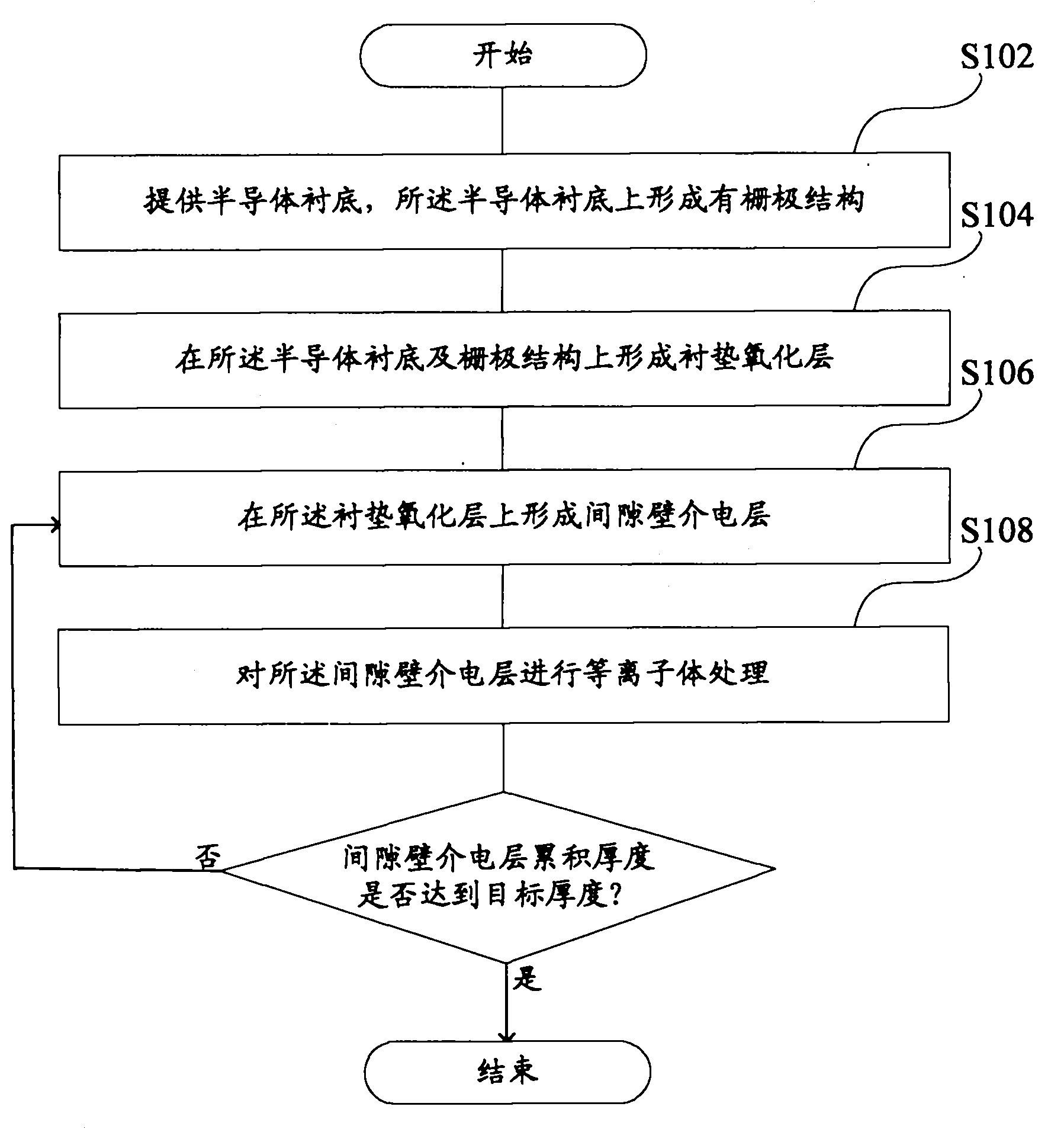
[0021] In order to make the above objects, features and advantages of the present invention more comprehensible, specific implementations of the present invention will be described in detail below in conjunction with the accompanying drawings.

[0022] In the following description, many specific details are set forth in order to fully understand the present invention, but the present invention can also be implemented in other ways than those described here, so the present invention is not limited by the specific embodiments disclosed below.

[0023] As described in the background technology section, when forming a spacer dielectric layer in the prior art MOS transistor manufacturing method, due to the loading effect of plasma enhanced chemical vapor deposition, the thickness of the spacer dielectric layer varies with the thickness of the semiconductor substrate. The variation of device density will have large process deviation, and the thickness deviation of the spacer dielectr...


PUM

PropertyMeasurementUnit
thicknessaaaaaaaaaa
thicknessaaaaaaaaaa
thicknessaaaaaaaaaa

Abstract

The invention provides a making method for a MOS (Metal Oxide Semiconductor) transistor. The making method comprises the following steps: providing a semiconductor substrate on which a gate structure is formed; forming a liner oxidation layer on the semiconductor substrate and the gate structure; forming a clearance wall dielectric layer on the liner oxidation layer; performing plasma treatment on the clearance wall dielectric layer; and repeating the formation process of the clearance wall dielectric layer and the formation process of the plasma treatment for at least one time until the accumulated thickness of the clearance wall dielectric layer reaches the target thickness. The making method for the MOS transistor provided by the invention reduces the thickness deviation of the MOS transistor clearance walls in different areas of the thickness of the devices on the semiconductor substrate, thus consistency in effective trench lengths of the MOS transistors can be improved and consistency in the performances of the MOS transistors can be further improved.

Description

technical field [0001] The present invention relates to the technical field of semiconductors, and more specifically, the present invention relates to a manufacturing method of a MOS transistor. Background technique [0002] With the continuous advancement of integrated circuits, that is, IC technology, the number of components integrated on the same chip has evolved from the initial tens of hundreds to the present millions. The performance and complexity of current ICs are far beyond what could have been imagined at the beginning. In order to meet the requirements of complexity and circuit density (ie: the number of devices integrated into a certain area), the minimum feature size, which is known as the "geometric line width" of the device, is getting smaller and smaller with the innovation of process technology. Today, the minimum line width of MOS transistors is less than 65 nanometers. [0003] With the continuous reduction of the minimum line width of MOS transistors,...

Claims


Application Information

Patent Timeline
Patent Type & Authority Applications(China)
IPC IPC(8): H01L21/336H01L21/28
Inventor 李敏
Owner SEMICON MFG INT (SHANGHAI) CORP
Why Eureka
Try Eureka