Low-loss silicon-based filter chip capable of improving reuse rate and manufacturing method thereof

A filter chip and manufacturing method technology, applied in semiconductor/solid-state device manufacturing, impedance network, electrical components, etc., can solve problems such as difficult multi-chip integration, low chip usage rate, large filter size, etc., to improve the reuse rate , easy integration, small size effect

Active Publication Date: 2020-07-17
昆山鸿永微波科技有限公司
View PDF3 Cites 1 Cited by
  • Summary
  • Abstract
  • Description
  • Claims
  • Application Information

AI Technical Summary

Problems solved by technology

[0004] The main technical problem to be solved by the present invention is to provide a low-loss silicon-based filter chip with improved reuse rate and its manufacturing method, so as to solve the problem that the existing traditional filter has a large volume and is difficult to realize multi-chip integration, and solve the existing Silicon-based filter chips have problems such as poor out-of-band rejection, high loss, and low chip utilization

Method used


Image

  • Low-loss silicon-based filter chip capable of improving reuse rate and manufacturing method thereof
  • Low-loss silicon-based filter chip capable of improving reuse rate and manufacturing method thereof
  • Low-loss silicon-based filter chip capable of improving reuse rate and manufacturing method thereof

Examples


Embodiment Construction

[0028] The following will clearly and completely describe the technical solutions in the embodiments of the present invention. Obviously, the described embodiments are only some of the embodiments of the present invention, rather than all the embodiments. Based on the embodiments of the present invention, all other embodiments obtained by persons of ordinary skill in the art without making creative efforts belong to the protection scope of the present invention.

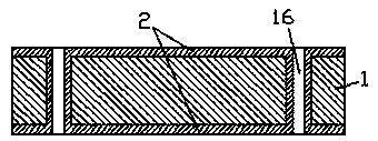
[0029] figure 1 It is a structural schematic diagram of an existing silicon-based filter chip, including a metal layer 2 and a dielectric layer 1, the metal layer 2 is arranged on the upper and lower surfaces of the dielectric layer 1, and the dielectric layer 1 is provided with a through hole 16;

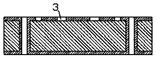
[0030] figure 2 is a structural schematic diagram of another existing silicon-based filter chip, in figure 1 On the basis of the silicon-based filter chip shown, a slot 3 is added on the metal layer above the dielectri...


PUM

PropertyMeasurementUnit
electrical resistivityaaaaaaaaaa
thicknessaaaaaaaaaa

Abstract

The invention discloses a low-loss silicon-based filter chip capable of improving reuse rate and a manufacturing method thereof. The silicon-based filter chip comprises a high-resistance silicon dielectric layer, a first metal layer, a second metal layer, a third metal layer and a fourth metal layer, the first metal layer is arranged on the top surface of the high-resistance silicon dielectric layer; a silicon cavity is formed in the bottom surface of the high-resistance silicon dielectric layer in a concave manner; the second metal layer is arranged in the silicon cavity; the third metal layer is arranged on the bottom surface of the high-resistance silicon dielectric layer and keeps away from the silicon cavity, the fourth metal layer is arranged on the bottom surface of the third metallayer, a through hole penetrating through the first metal layer upwards is formed in the high-resistance silicon dielectric layer, a metal deposition layer is arranged on the inner wall of the throughhole, and production is carried out through etching and micromachining processes. With application of the mode, the low-loss silicon-based filter chip capable of improving the reuse rate and the manufacturing method thereof are convenient to produce, the out-of-band rejection degree of the silicon-based filter chip is improved, loss is reduced and the reuse rate is high.

Description

technical field [0001] The invention relates to the field of filter circuits, in particular to a low-loss silicon-based filter chip with improved reusability and a manufacturing method thereof. Background technique [0002] Filters play an important role in frequency selective filtering in microwave and millimeter wave systems. Specifically, filters allow electrical signals of a certain frequency to pass through while blocking electrical signals of other frequencies. The main performance indicators of filters include insertion loss, bandwidth, out-of-band selectivity, and circuit size. Widening bandwidth, improving out-of-band rejection, and circuit miniaturization have always been the key design difficulties of filters. [0003] Traditional filters include cavity filters, LC filters and planar filters. The cavity filter is formed by cutting metal as a whole, the LC filter is composed of a combination of inductors, capacitors and resistors, and the planar filter is composed ...

Claims


Application Information

Patent Timeline
Patent Type & Authority Applications(China)
IPC IPC(8): H01L23/48H01L23/535H01L21/768H03H3/007H03H3/02
CPCH01L23/535H01L23/481H01L21/76838H01L21/7685H03H3/0073H03H3/0075H03H3/02H03H2003/027H03H2003/028Y02D30/70
Inventor 万晶梁晓新
Owner 昆山鸿永微波科技有限公司
Why Eureka
Try Eureka