Method of polishing thin film formed on substrate

a thin film and substrate technology, applied in the direction of optical radiation measurement, lapping machines, instruments, etc., can solve the problem of not being able to determine the thickness of the film

Active Publication Date: 2007-08-28
EBARA CORP
View PDF11 Cites 5 Cited by
  • Summary
  • Abstract
  • Description
  • Claims
  • Application Information

AI Technical Summary

Benefits of technology

[0009]The present invention has been made in view of the above drawbacks. An object of the present invention is to accurately determine a thickness of a thin film of copper or other material formed on a substrate using ellipsometry so as to properly polish the thin film on the substrate.
[0015]As described above, in the present invention, the thin film, which is actually formed on the substrate, is polished by the CMP process, so that the oxide film is removed. Thereafter, the substrate is cleaned, and ellipsometry is then performed to measure the thickness of the thin film and the oxide film which is formed on the thin film after cleaning. Therefore, the film thickness can be measured very accurately, and hence the CMP processing of the thin film can be performed properly.

Problems solved by technology

However, with respect to the copper thin film formed on the substrate in an IC chip fabrication process or other process, it has been found that it is not appropriate to determine the film thickness by such ellipsometry using the optical constant of copper which is published in handbooks, documents, and the like. FIG. 1 shows this fact.

Method used


Image

  • Method of polishing thin film formed on substrate
  • Method of polishing thin film formed on substrate
  • Method of polishing thin film formed on substrate

Examples


Embodiment Construction

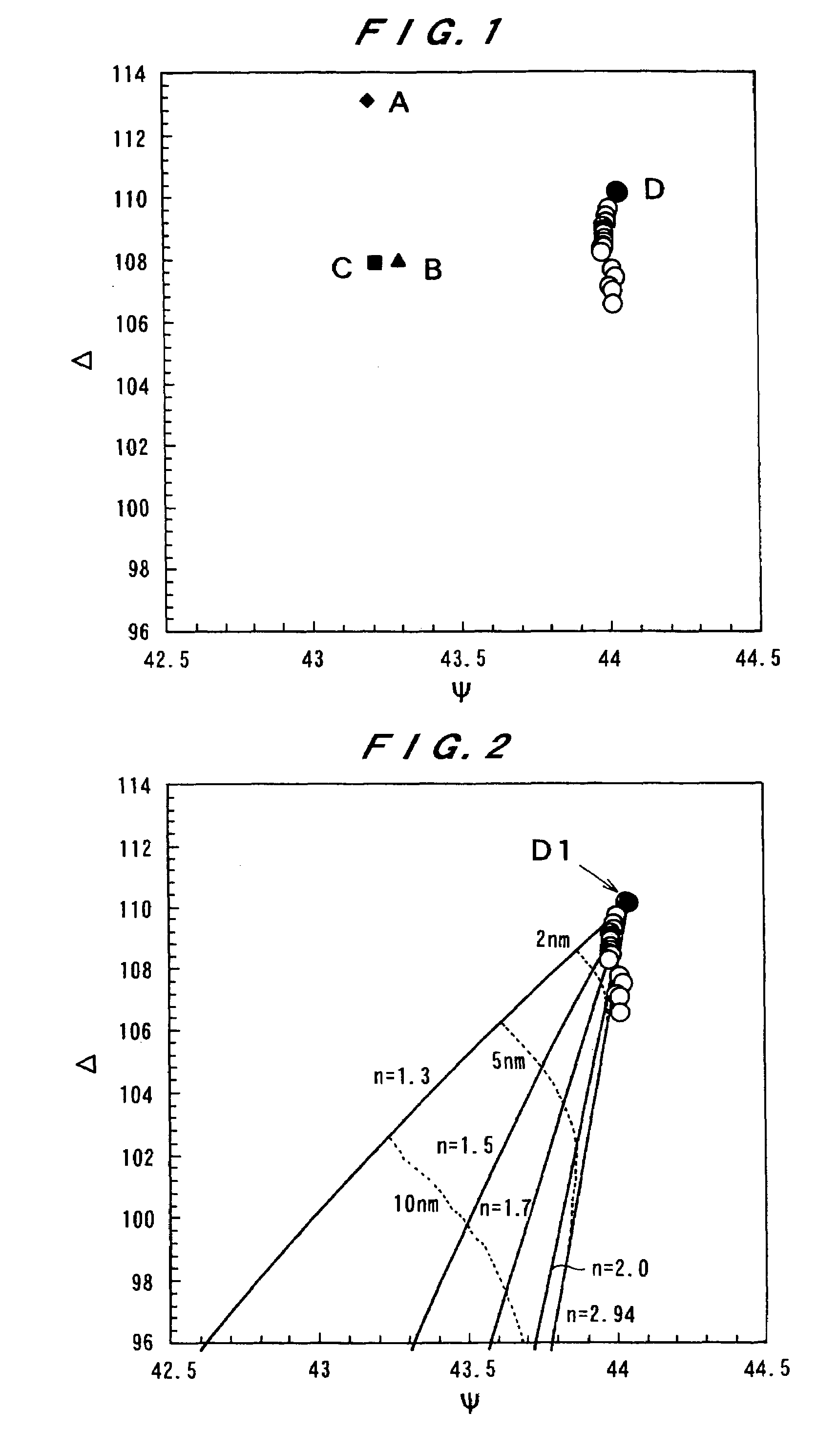
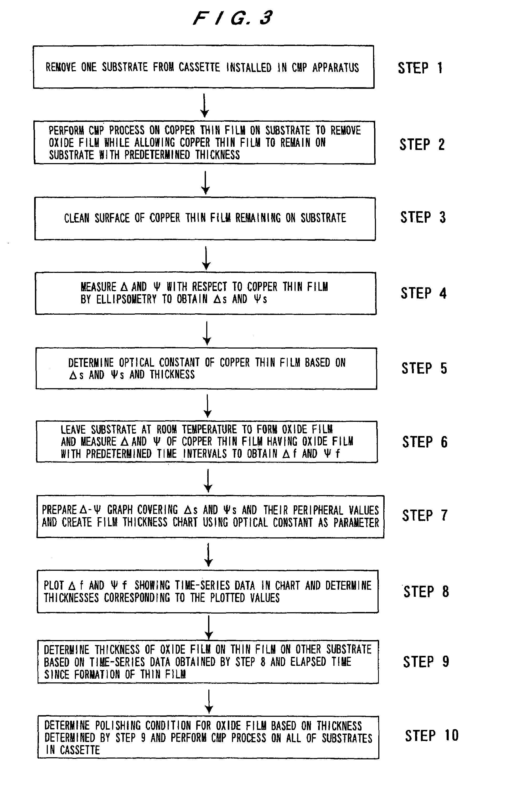
[0023]A polishing method according to an embodiment of the present invention will be described with reference to the drawings. The polishing method of the present invention is performed with a CMP apparatus, i.e., a chemical mechanical planarization apparatus. The CMP apparatus comprises at least one cassette in which a plurality of substrates, each having a film of copper or other material, are accommodated. The substrates are sequentially removed from the cassette and delivered to a turntable (polishing table). Each substrate is pressed against a polishing pad attached to the turntable and is thus polished to have a flat surface. The substrate, which has been planarized, is returned to the cassette via a cleaning station, a drying station, and other equipment.

[0024]The polishing method according to the embodiment of the present invention is designed to enable a CMP process, i.e., a chemical mechanical planarization process, to be performed properly. Specifically, this method perfo...


PUM

PropertyMeasurementUnit
Δaaaaaaaaaa
physical propertyaaaaaaaaaa
thicknessaaaaaaaaaa

Abstract

A method for polishing a thin film formed on a substrate includes planarizing a thin film formed on a reference substrate by a CMP process such that the thin film remains on the reference substrate. After the planarizing, the thin film is cleaned, and then values of Δ and Ψ with respect to the cleaned thin film are measured by ellipsometry. A physical property of the thin film is determined based on the Δ and Ψ which have been measured by ellipsometry, and a polishing condition for an other substrate having a thin film to be polished is set based on physical property data which are obtained by the determining of the physical property.

Description

BACKGROUND OF THE INVENTION[0001]1. Field of the Invention[0002]The present invention relates to a method of polishing a thin film formed on a substrate, and more particularly to a polishing method which can properly polish a thin film by determining a physical property and a thickness of the thin film utilizing ellipsometry.[0003]2. Description of the Related Art[0004]Ellipsometry is a method of determining the refractive index of a specimen by emitting polarized light to a flat surface of the specimen and measuring a change in the polarization state of reflected light. Ellipsometry is also used for determining a thickness of a thin film formed on a surface of a specimen.[0005]Fabrication processes of an IC chip include a process of forming thin films of several kinds of materials on a substrate (e.g., Si substrate) and a process of removing the thin films using CMP (i.e., chemical mechanical planarization). In a case of a copper thin film, for example, an oxide film such as CuO or...

Claims


Application Information

Patent Timeline
Patent Type & Authority Patents(United States)
IPC IPC(8): G01J4/00H01L21/304B24B49/03B24B49/12G01B11/06G01N21/21
CPCB24B37/042B24B49/03B24B49/12G01B11/0641G01N21/211
Inventor SHIMA, SHOHEIFUKUNAGA, AKIRA
Owner EBARA CORP
Why Eureka
Try Eureka