Address decoding

a decoding and address technology, applied in the field of address decoding, can solve the problems of reducing the overall performance of the data processing apparatus to unacceptable levels, and invalid address signals being provided to the address decoder

Active Publication Date: 2007-08-28
RGT UNIV OF MICHIGAN +1
View PDF6 Cites 4 Cited by
  • Summary
  • Abstract
  • Description
  • Claims
  • Application Information

AI Technical Summary

Benefits of technology

[0012]According to one aspect of the present invention there is provided a signal interface for interfacing with an address decoder, the signal interface comprising: a signal capture element operable to receive an address portion signal associated with a read access to a memory and to provide a first interim address portion signal and a second interim address portion signal, the signal capture element being operable during a pre-charged period to provide a first pre-charged logic level as the first interim address portion signal and the first pre-charged logic level as the second interim address portion signal, the signal capture element being further operable during an evaluate period to output an address portion logic level representative of the address portion signal as the first interim address portion signal and an inverted address portion logic level representative of an inverted address portion signal as the second interim address portion signal; and an inverter circuit operable to receive the first interim address portion signal and the second interim address portion signal from which a first address portion signal and a second address portion signal is respectively derived, the inverter circuit being operable during the pre-charged period to output to an address decoder a second pre-charged logic level as the first address portion signal and the second pre-charged logic level as the second address portion signal, the receipt of the first address portion signal and the second address portion signal at the second pre-charged logic level causing the address decoder to be prevented from causing a data access to the memory from occurring, the inverter circuit having transfer characteristics which cause the first address portion signal and the second address portion signal to be maintained at voltage levels interpreted by the address decoder as being the second pre-charged logic level should the first interim address portion signal or the second interim address portion signal fail to transition to a valid logic level during the evaluate period.
[0017]Maintaining the address portion signals provided to the address decoder during the evaluate period at voltage levels interpreted by the address decoder as being the second pre-charged logic level causes the address decoder to operate in a manner equivalent to that during the pre-charge period and prevents the address decoder from selecting multiple word lines. As a consequence, no corruption in the state stored in the memory can result due to the inadvertent flow of charge between cells in different rows of the memory.
[0018]Accordingly, it remains possible to utilise existing typical arrays of RAM cells, without modification, even in data processing apparatuses in which set-up and hold times are not observed and where metastability may occur. Furthermore, by avoiding the need to place read accesses to the memory in a read queue in an equivalent manner to write accesses avoids the introduction of delays when retrieving data.
[0026]In embodiments, receipt of the first address portion signal and the second address portion signal at the second pre-charged logic level causes the address decoder to be prevented from activating data selection circuitry in a memory.
[0027]According to a second aspect of the present invention there is provided a method of interfacing with an address decoder, comprising the steps of: receiving an address portion signal associated with a data access to a memory and providing a first interim address portion signal and a second interim address portion signal; providing, during a pre-charged period, a first pre-charged logic level as the first interim address portion signal and the first pre-charged logic level as the second interim address portion signal; outputting, during an evaluate period, an address portion logic level representative of the address portion signal as the first interim address portion signal and an inverted address portion logic level representative of an inverted address portion signal as the second interim address portion signal; and receiving the first interim address portion signal and the second interim address portion signal from which a first address portion signal and a second address portion signal is respectively derived; outputting to an address decoder, during the pre-charged period, a second pre-charged logic level as the first address portion signal and the second pre-charged logic level as the second address portion signal, the receipt of the first address portion signal and the second address portion signal at the second pre-charged logic level causing the address decoder to be prevented from causing a data access to the memory from occurring; and causing the first address portion signal and the second address portion signal to be maintained at voltage levels interpreted by the address decoder as being the second pre-charged logic level should the first interim address portion signal or the second interim address portion signal fail to transition to a valid logic level during the evaluate period.
[0028]According to a third aspect of the present invention there is provided a memory decoder comprising: a signal capture element for receiving an address portion signal associated with a data access to a memory, for providing a first interim address portion signal and a second interim address portion signal, for providing during a pre-charged period, a first pre-charged logic level as the first interim address portion signal and the first pre-charged logic level as the second interim address portion signal and for outputting during an evaluate period an address portion logic level representative of the address portion signal as the first interim address portion signal and an inverted address portion logic level representative of an inverted address portion signal as the second interim address portion signal; and an inverter circuit operable for receiving the first interim address portion signal and the second interim address portion signal from which a first address portion signal and a second address portion signal is respectively derived, for outputting to an address decoder during the pre-charged period a second pre-charged logic level as the first address portion signal and the second pre-charged logic level as the second address portion signal, the receipt of the first address portion signal and the second address portion signal at the second pre-charged logic level causing the address decoder to be prevented from causing a data access to the memory from occurring, the inverter circuit having transfer characteristics for causing the first address portion signal and the second address portion signal to be maintained at voltage levels interpreted by the address decoder as being the second pre-charged logic level should the first interim address portion signal or the second interim address portion signal fail to transition to a valid logic level during the evaluate period.

Problems solved by technology

This is because read accesses tend to be on the critical path due to the long latency computations required to determine the address values of the data to be read and introducing such delays would adversely reduce the overall performance of the data processing apparatus to unacceptable levels.
This is because metastability can result in invalid address signals being provided to the address decoder.
These metastable signals can result in invalid address signals being provided because the metastable signals can be interpreted as being at two different logic levels.
Such invalid signals may then be directly driven onto the word lines in the memory and could result in the selection of multiple word lines.
In a typical memory, selecting multiple word lines simultaneously during a read access can cause a corruption in the state stored in the memory due to the inadvertent flow of charge between cells in different rows of the memory.
However, as also mentioned above, in the scenario where metastable signals may be generated, observing such timing constraints cannot be guaranteed.

Method used


Image

  • Address decoding
  • Address decoding
  • Address decoding

Examples


Embodiment Construction

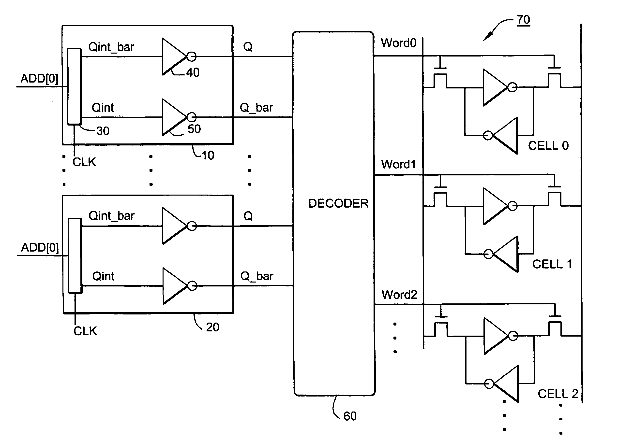
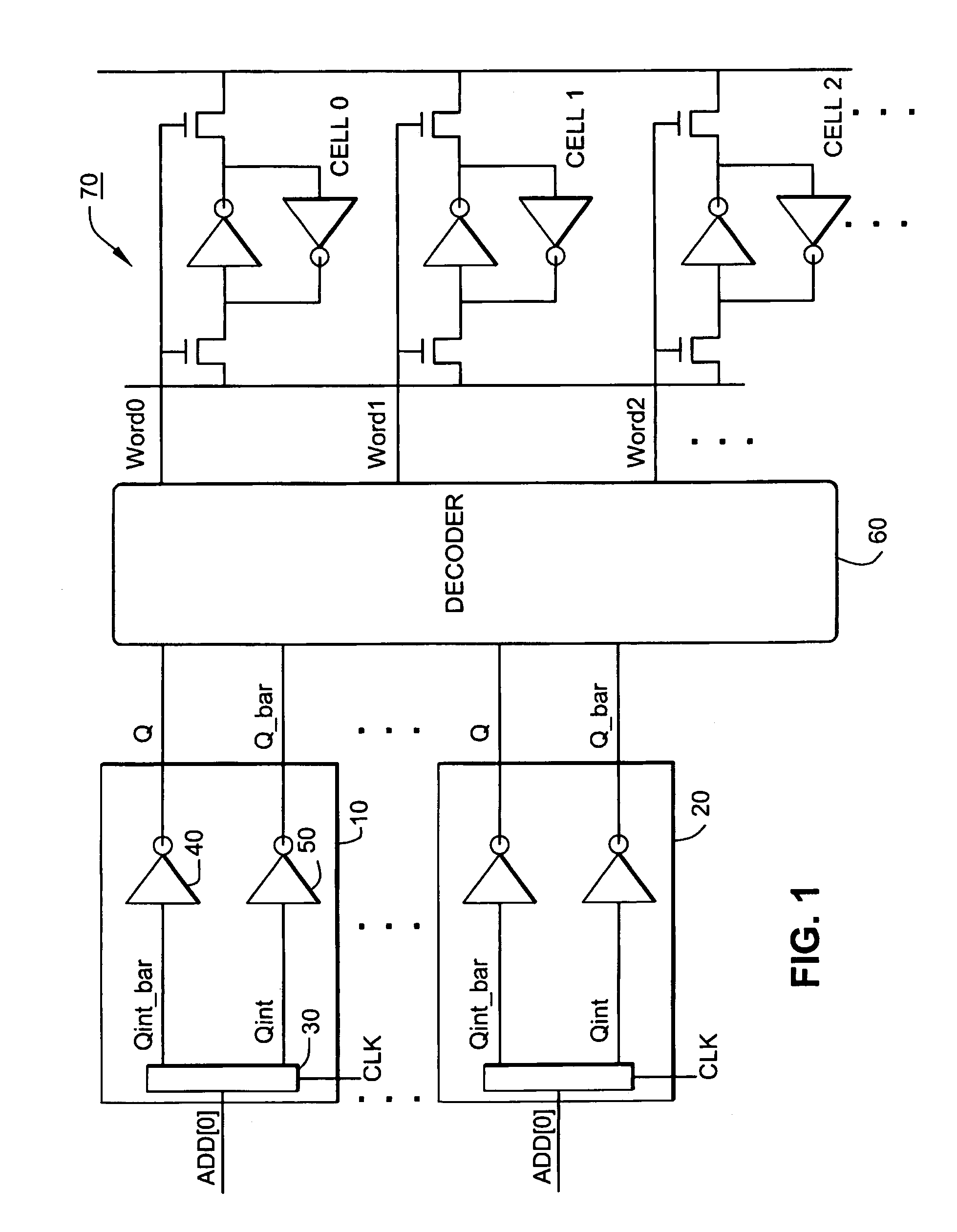
[0036]FIG. 1 illustrates a number of signal interfaces 10, 20 according to an embodiment of the present invention, each operable to interface with an address decoder 60 and a memory 70.

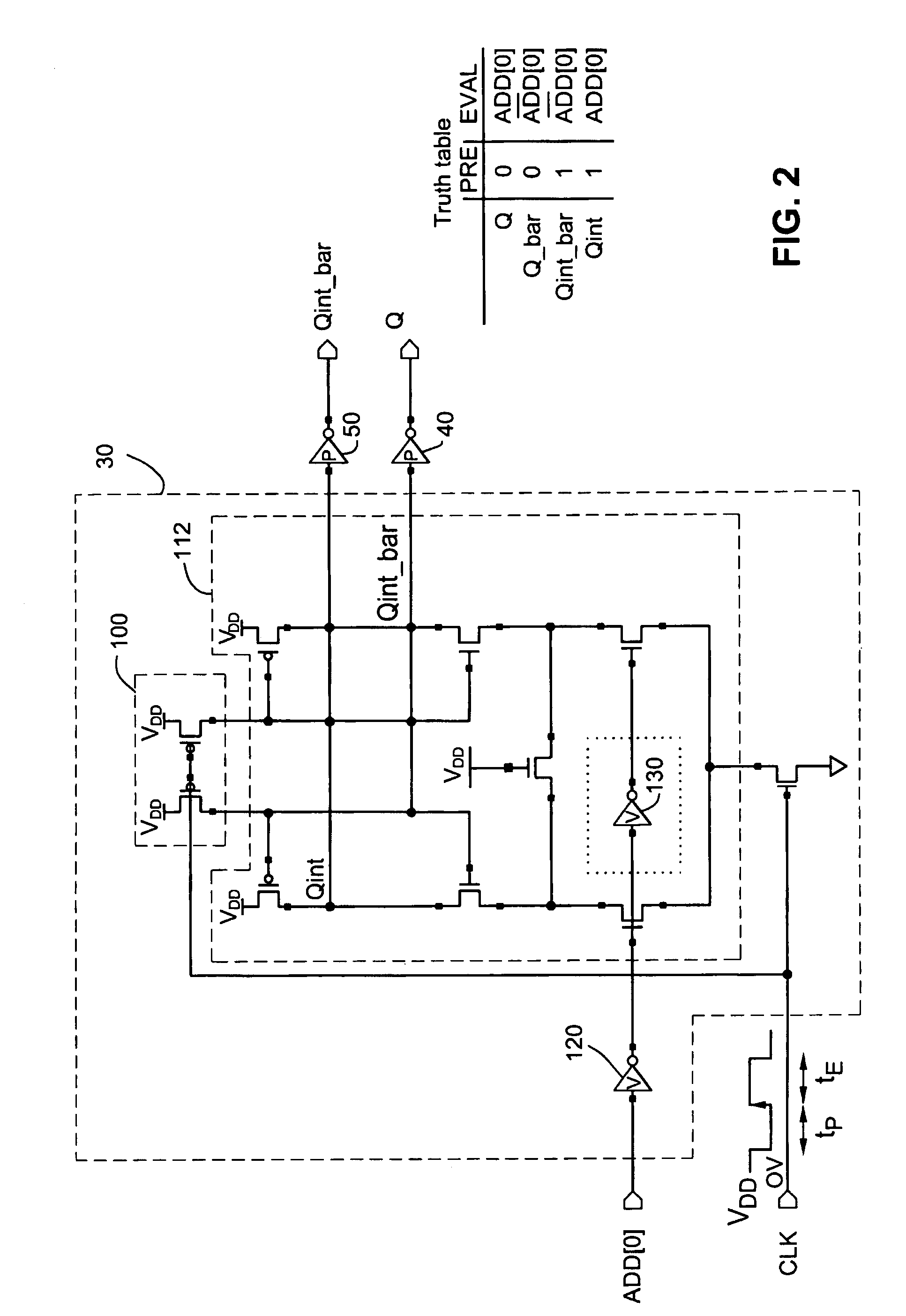
[0037]Each signal interface 10, 20 comprise a precharge / evaluate circuit 30 and inverters 40 and 50. As will be explained in more detail below, the characteristics of these inverters 40 and 50 are selected to enable the associated signal interface to receive metastable signals whilst ensuring that no data corruption occurs in the memory 70. Each precharge / evaluate circuit 30 receives a portion of an address signal relating to an address to be accessed in the memory 70. In this embodiment, signal interface 10 receives bit 0 (ADD[0]) of the address value to be accessed in the memory 70, another signal interface receives bit 1 (ADD[1]) of the address value to be accessed in the memory 70, signal interface 20 receives bit n (ADD[n]) of the address value to be accessed in the memory 70, and so on.

[0038]Eac...


PUM


Abstract

A signal capture element for providing a first pre-charged logic level as first and second interim address portion signals during a pre-charged period and outputting during an evaluate period an address portion logic level as the first interim address portion signal and an inverted address portion logic level as the second interim address portion signal. First and second address portion signals are derivable respectively from first and second interim address portion signals. An inverter circuit for outputting to an address decoder during a pre-charged period a second pre-charged logic level as the first and second address portion signals. The inverter circuit having transfer characteristics that maintain voltage levels such that the first and second address portion signals are interpreted to be at the second pre-charged logic level despite the first or second interim address portion signal failing to transition to a valid logic level during the evaluate period.

Description

BACKGROUND OF THE INVENTION[0001]1. Field of the Invention[0002]The present invention relates to address decoding. Embodiments of the present invention relate to a circuit for driving an address decoder which is tolerant of metastable signals.[0003]2. Description of the Prior Art[0004]In a data processing apparatus, such as a pipelined data processing apparatus, a series of serially connected stages are formed. The processing circuitry of each processing stage is responsive to input signals received from preceding processing stages in the pipeline or from elsewhere and generates output signals. Between each stage of the pipeline is provided a signal capture element such as a latch or a sense amplifier into which one or more signal values are stored. The latch receives the input signals, stores the input signal value and presents this stored value on its output in response to a clock signal provided thereto.[0005]In order for the latch to reliably store the input signals provided at ...

Claims


Application Information

Patent Timeline
Patent Type & Authority Patents(United States)
IPC IPC(8): G11C7/00G11C8/00
CPCG11C8/08G11C8/10G11C11/418
Inventor BLAAUW, DAVID THEODOREBULL, DAVID MICHAELDAS, SHIDHARTHA
Owner RGT UNIV OF MICHIGAN
Why Eureka
Try Eureka