

CCD imager constructed with CMOS fabrication techniques and back illuminated imager with improved light capture
a cmos fabrication and imager technology, applied in the field of semiconductor circuit design of optical sensors and ccd sensor arrays, can solve problems such as difficult integration of ccd imagers with cmos process peripheral circuitry, blunders and related image artifacts,
- Summary
- Abstract
- Description
- Claims
- Application Information
AI Technical Summary
Problems solved by technology
Method used
Image

Examples
Embodiment Construction
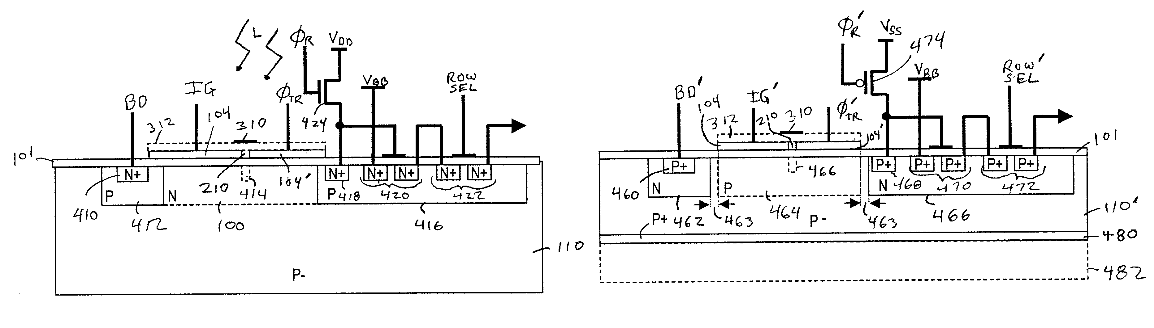
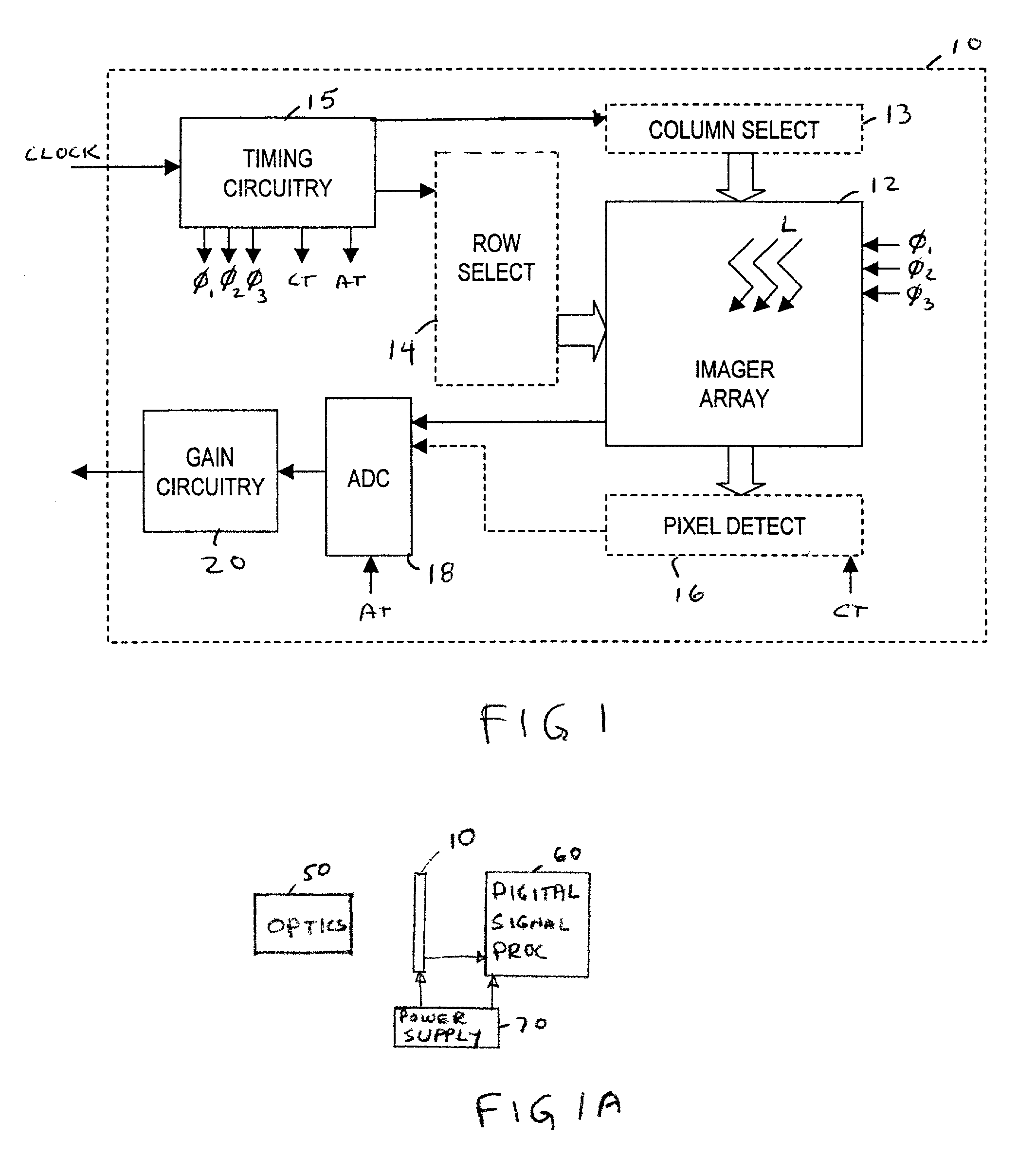
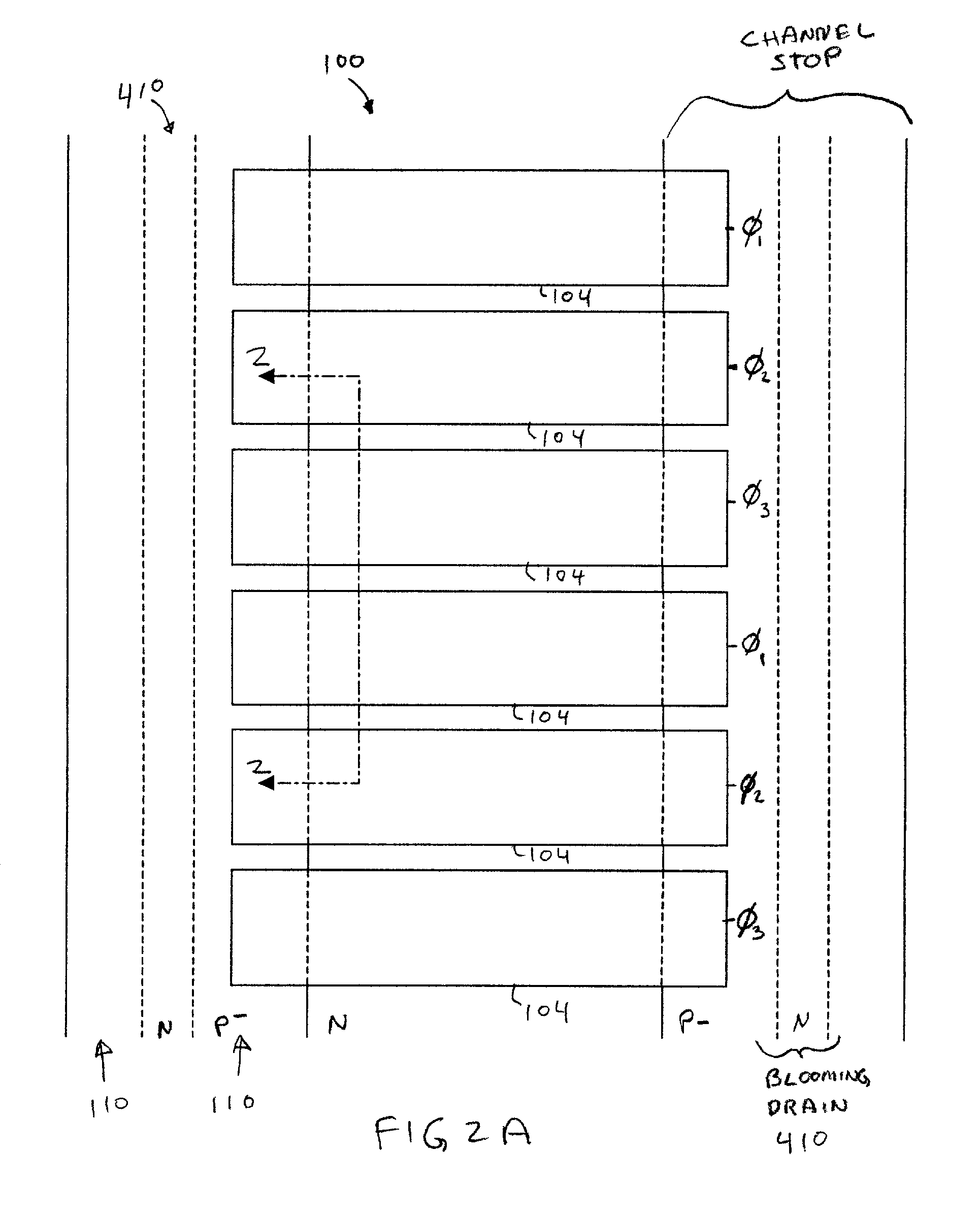
[0026]The invention is described in terms of exemplary embodiments which are illustrated in the drawing figures. The drawing figures are not to scale. Indeed, dimensions of the drawing figures are exaggerated to aid in the description of the invention.
[0027]Certain terminology used in the following description is for convenience only and is not limiting. The term “standard CMOS IC fabrication processes”, is used to describe processes which are compatible with standard CMOS IC fabrication processes, that is to say, processes using fabrication steps that are commonly used in CMOS IC fabrication facilities including optional process steps such as threshold adjusting diffusions. In such processes, devices which are easily fabricated with CMOS IC fabrication processes can be formed on a substrate or semiconductor “wafer” along with the desired imaging devices in accordance with the present invention. In the drawings, the same reference numerals are used for designating the same elements ...
PUM
 Abstract
Description
Claims
Application Information