Stackable single package and stacked multi-chip assembly

a single package and chip technology, applied in the field of packaged components, can solve the problems of silicon chip damage, chips have a comparatively large height, and more costs of the assembling process

Inactive Publication Date: 2007-09-04
POLARIS INNOVATIONS LTD
View PDF11 Cites 13 Cited by
  • Summary
  • Abstract
  • Description
  • Claims
  • Application Information

AI Technical Summary

Benefits of technology

[0011]In another aspect, the invention prevents any risk of damages during handling procedures of the chips during the assembling process.
[0012]In yet another aspect, the invention simplifies the assembling process and increases the reliability of the microelectronic package by eliminating any wire bond process.
[0022]Moreover, the mold ring enables the stacked assembly to be very thin.

Problems solved by technology

It seems to be clear that the necessity of chips with different dimensions leads to more costs for the assembling process since the mounting tools must be able to mount chips with different outer dimensions.
Such a stack of chips has a comparatively big height, which is contrary to the recent development to produce chip assemblies with a very low height.
The total height of such assemblies can be reduced in limitations by thinning the chips before assembling them in a stack but this produces the risk of silicon chip damages during transportation and test handling and assembling on bare chip package construction.
Especially the edges of the chips are very sensitive.
This is not suitable for protecting the chip during handling on the assembling process.
Also, it is not possible to use the encapsulant as a carrier for contact elements or a reroute layer.

Method used


Image

  • Stackable single package and stacked multi-chip assembly
  • Stackable single package and stacked multi-chip assembly
  • Stackable single package and stacked multi-chip assembly

Examples


Embodiment Construction

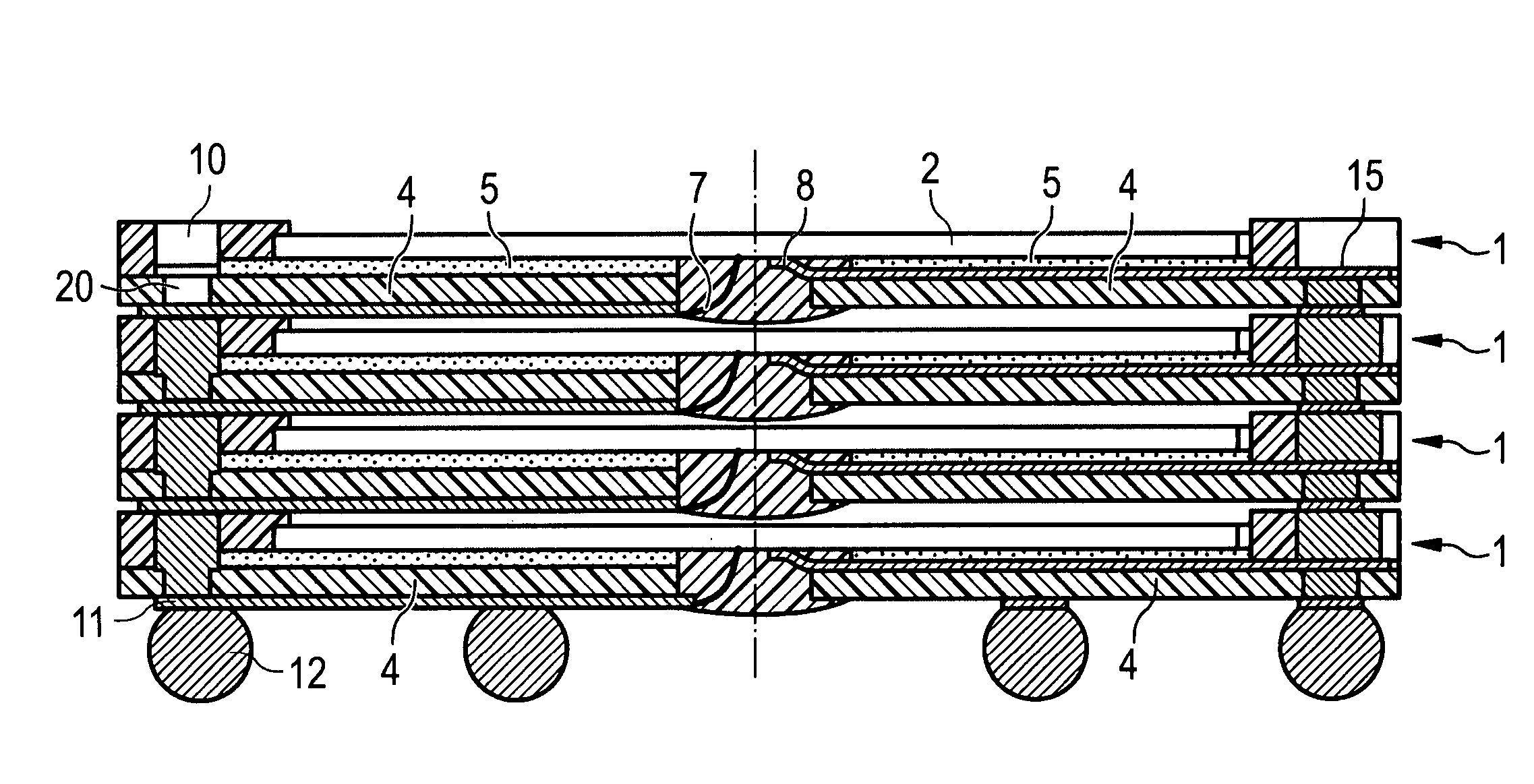
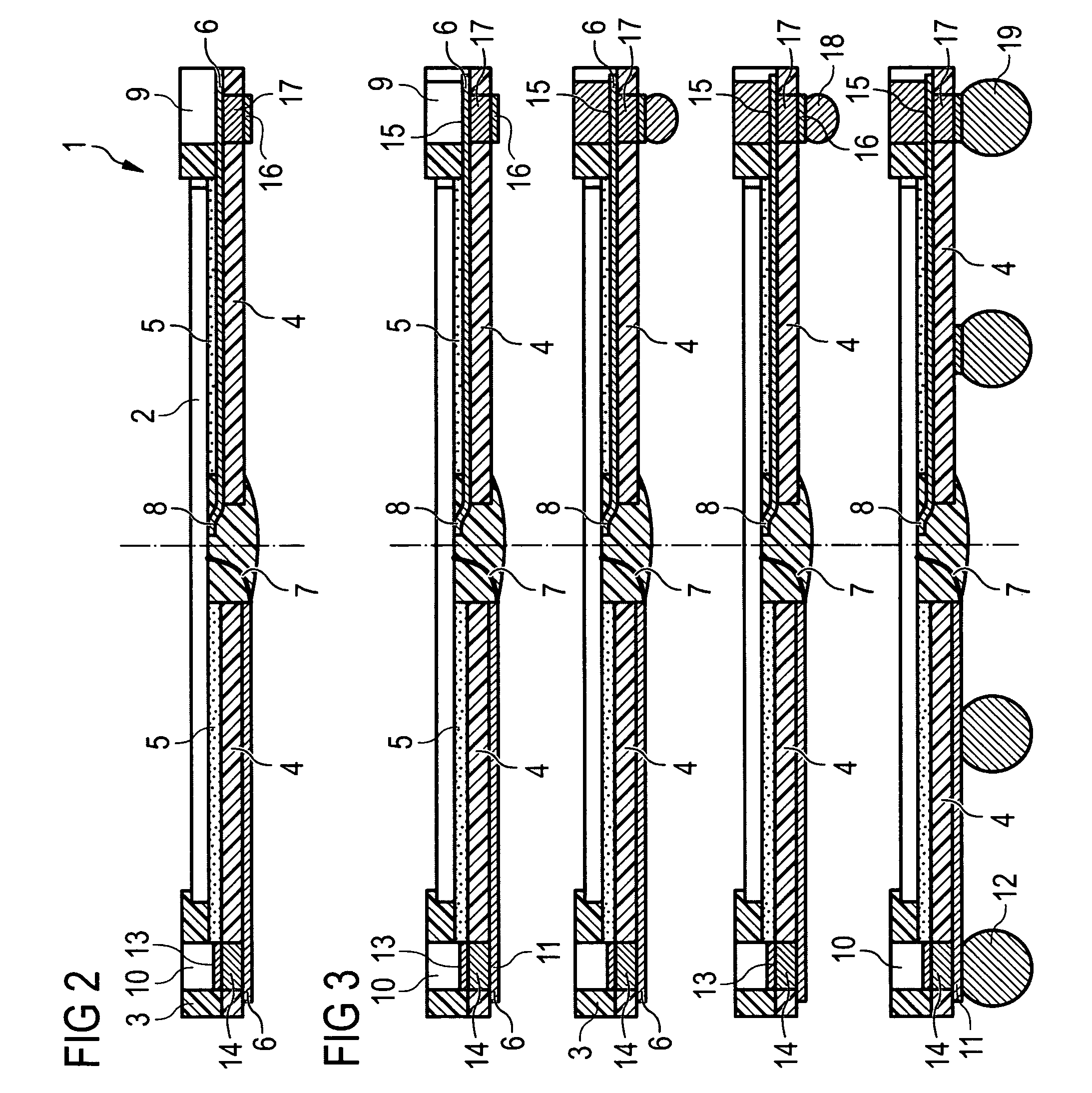
[0030]FIG. 1 illustrates a schematic top view of a single package 1 according to embodiments of the invention. The core of the single package 1 is a chip 2, also called a die, surrounded by a mold ring 3.

[0031]The mold ring 3 has at least two functions, which are first protecting the corner and edge of the chip 2 and second it serves as a means to realize electrical interconnections between stacked single package 1 chips as will be explained later. Referring also to FIG. 2, the chip 2 is mounted on a substrate 4 by die bonding with an adhesive tape 5. The substrate 4 (e.g., single layer substrate) is provided with a copper wiring 6 either on the surface opposite to the chip 2 mounting side or on the chip 2 mounting side.

[0032]Therefore, the left side of FIG. 2 illustrates a wiring 6 on the side opposite the chip 2 mounting side. In this case the wiring 6 of the substrate 4 is connected with respective bond pads on the chip 2 with wire loops 7 performed by well-known technology of wi...


PUM


Abstract

A stackable packaged chip includes a substrate with a conductive wiring formed therein or thereon. The substrate further includes a plurality of substrate contact pads arranged around a periphery portion of the substrate. A chip mounted on the substrate including contact pads that are electrically connected with the conductive wiring of the substrate, and a ring surrounding edges of the chip are also included. The ring is formed from an electrically insulating material and includes a plurality of openings, each opening adjacent a substrate contact pad to allow for electrical connection to the chip though the substrate contact pad.

Description

TECHNICAL FIELD[0001]The invention relates generally to packaged components and in particular embodiments to a stackable single package and a stacked multi-chip assembly.BACKGROUND[0002]There are many well-known microelectronic packages with stacked chips within a housing, e.g., made of a mold compound. The chips, also called silicon dies, are stacked face up or face down with an adhesive and are electrically connected with a base substrate via wire loops. An example of a stacked chip assembly on a substrate is known from U.S. Patent Publication No. 2003 / 0159773 A1, which is incorporated herein by reference. There are chips with different dimensions mounted one over another such that the chip with the smaller dimensions is mounted on a chip with larger dimensions. Between the chips is arranged an adhesive. A chip with smaller dimensions must be mounted on a base chip because the rim portion of the base chip is provided with bond pads for electrical connections. These bond pads are c...

Claims


Application Information

Patent Timeline
Patent Type & Authority Patents(United States)
IPC IPC(8): H01L23/02H01L21/00
CPCH01L23/3128H01L25/105H01L2924/15311H01L24/48H01L2224/4824H01L2224/73221H01L2924/10253H01L2225/1058H01L2224/50H01L2924/00H01L2924/00014
Inventor REISS, WERNERHETZEL, WOLFGANG
Owner POLARIS INNOVATIONS LTD
Why Eureka
Try Eureka