Semiconductor device with a high thermal dissipation efficiency

a technology of semiconductor devices, which is applied in the direction of semiconductor devices, semiconductor/solid-state device details, electrical apparatus, etc., can solve the problems of reduced heat dissipation efficiency, increased heat dissipation, and restricted reworkability in the case of defects or insufficient thermal connections, etc., to achieve good mechanical stability and high thermal dissipation efficiency

Active Publication Date: 2007-09-18
GLOBALFOUNDRIES US INC
View PDF4 Cites 18 Cited by
  • Summary
  • Abstract
  • Description
  • Claims
  • Application Information

AI Technical Summary

Benefits of technology

[0009]It is an aspect of the present invention to provide a semiconductor device having a high thermal dissipation efficiency and a good mechanical stability, which is compatible to the existing semiconductor process technology and which provides the possibility of re-working in case of defects.
[0010]Another aspect of the present invention is to provide a method for fabricating a semiconductor device having a high thermal dissipation efficiency with minimal induction of stress to the semiconductor device (well below fracture strength of the device), even if different materials are used.
[0012]In an advantageous embodiment of the present invention, the semiconductor device further comprises a manifold layer attached to the thermally conducting structure. By using a manifold layer, it is possible to supply a cooling liquid or water to the structural elements of the thermally conducting structure. Thereby, a very high cooling efficiency of the semiconductor device can be obtained.
[0013]In another advantageous embodiment of the present invention, the semiconductor device is integrated into a device for jet impingement cooling. Due to the fact that the surface of the semiconductor device is enlarged by the thermally conducting structure, a good cooling performance of the semiconductor device can be achieved.

Problems solved by technology

As a consequence, there arises the problem of increased heat dissipation due to the increase in power density.
One disadvantage of this multi-chip module is that the heat transferred from the semiconductor chips to the air has to pass three boundary layers, so that the heat dissipation efficiency is reduced.
Besides, the reworkability in case of defects or insufficient thermal connections is restricted due to the encapsulation of the thermally conductive blocks, the semiconductor chips and the substrate with the resin package body.
Furthermore, in general air cooling approaches are quickly reaching their limits.
The disadvantage of these cooling methods consists in the connection of liquid coolers to the surfaces of the semiconductor chips.
In order to level out roughness and warp, a thick thermally interface between the chips and the liquid coolers is required which causes a high thermally resistance that deteriorates the cooling performance.
However, the cooling efficiency of jet impingement coolers is generally low due to the unstructured only flat impingement surface of the semiconductor chips.
A drawback of this method is that surface enlargement of processor chips by deep trench etching of wafers causes yield reduction, either due to the deep trench etch process stability or due to mechanical fracture of the patterned surface.
Therefore, the method is cost ineffective.
Moreover, deep trench backside etching of wafers can cause process compatibility issue problems, does not allow a re-working of this process in case of defects and makes the semiconductor chips more fragile to breaking.
As a consequence, such etching processes are not accepted in chip manufacturing.

Method used


Image

  • Semiconductor device with a high thermal dissipation efficiency
  • Semiconductor device with a high thermal dissipation efficiency
  • Semiconductor device with a high thermal dissipation efficiency

Examples


first embodiment

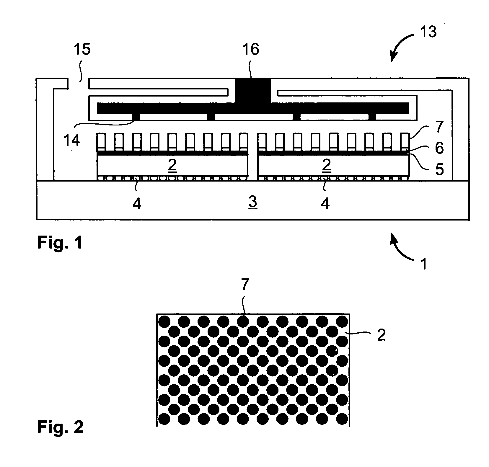
[0047]FIG. 1 shows a multi-chip module 1, according to the present invention in a cross-sectional view, which is integrated into a device for jet impingement cooling 13. The multi-chip module 1 comprises a common substrate 3 carrying a multilayer interconnection structure thereon and two semiconductor chips 2 attached to the surface of the substrate 3 in a face-down state via solder balls 4. The semiconductor chips 2 are mounted onto the surface of the substrate 3 by a flip chip process such as the common C4 technology process.

[0048]Each of the semiconductor chips 2 comprises an adhesion layer 5 coating the backsides of the semiconductor chips 2. The adhesion layers 5 consist for example of nickel and gold.

[0049]The multi-chip module 1 further comprises a thermally conducting structure comprising an array of free-standing studs 7 attached to the adhesion layers 5 of the semiconductor chips 2 via solder bonds 6. The studs 7 are essentially formed of a thermally conducting material su...

second embodiment

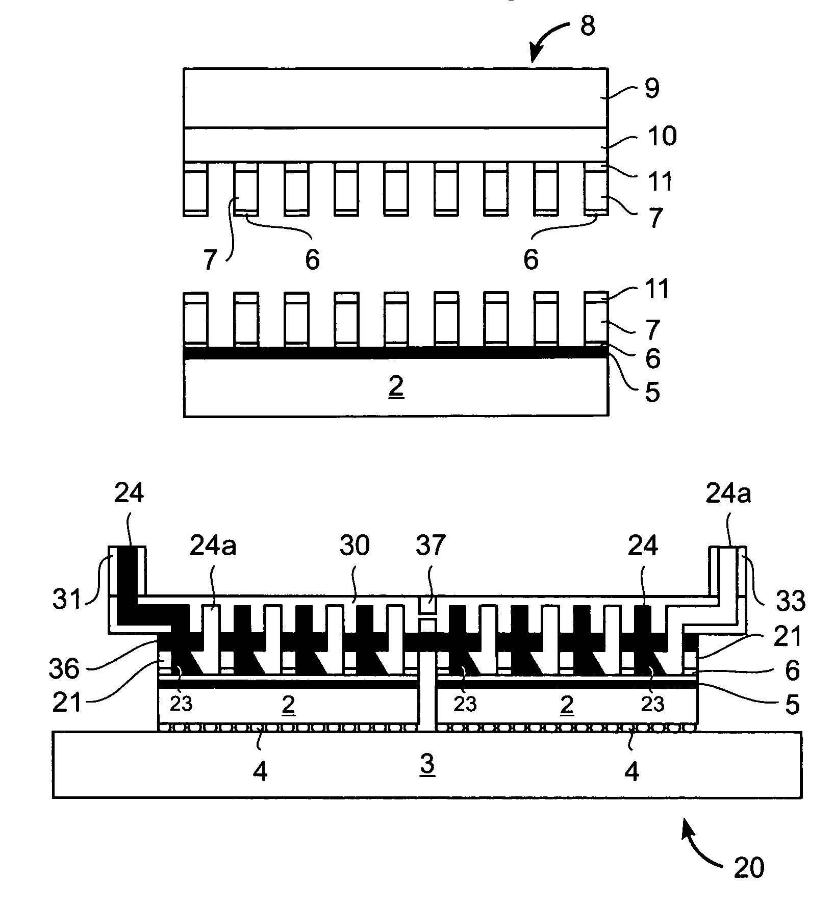
[0062]Instead of integrating a multi-chip module 1 into a device for jet impingement cooling 13, the multi-chip module 1 and the semiconductor chips, respectively, can also be provided with micro channel or duct cooling. In this regard, FIG. 4 illustrates, in a cross-sectional view, a multi-chip module 20 according to the present invention. This multi-chip module 20 also comprises two semiconductor chips 2 attached to the upper surface of a common substrate 3 in the face-down state via solder balls 4. The backsides of the semiconductor chips 2 are again each covered with an adhesion layer 5.

[0063]Instead of free-standing studs, the multi-chip module 20 further comprises two grids 21 of connected fins attached to each of the backsides of the semiconductor chips 2 for surface enlargement. These grids 21, which comprise a thermally conducting material such as copper, are bonded to the adhesion layers 5 coating the backsides of the chips 2 via solder bonds 6.

[0064]For this, FIG. 5 depic...

third embodiment

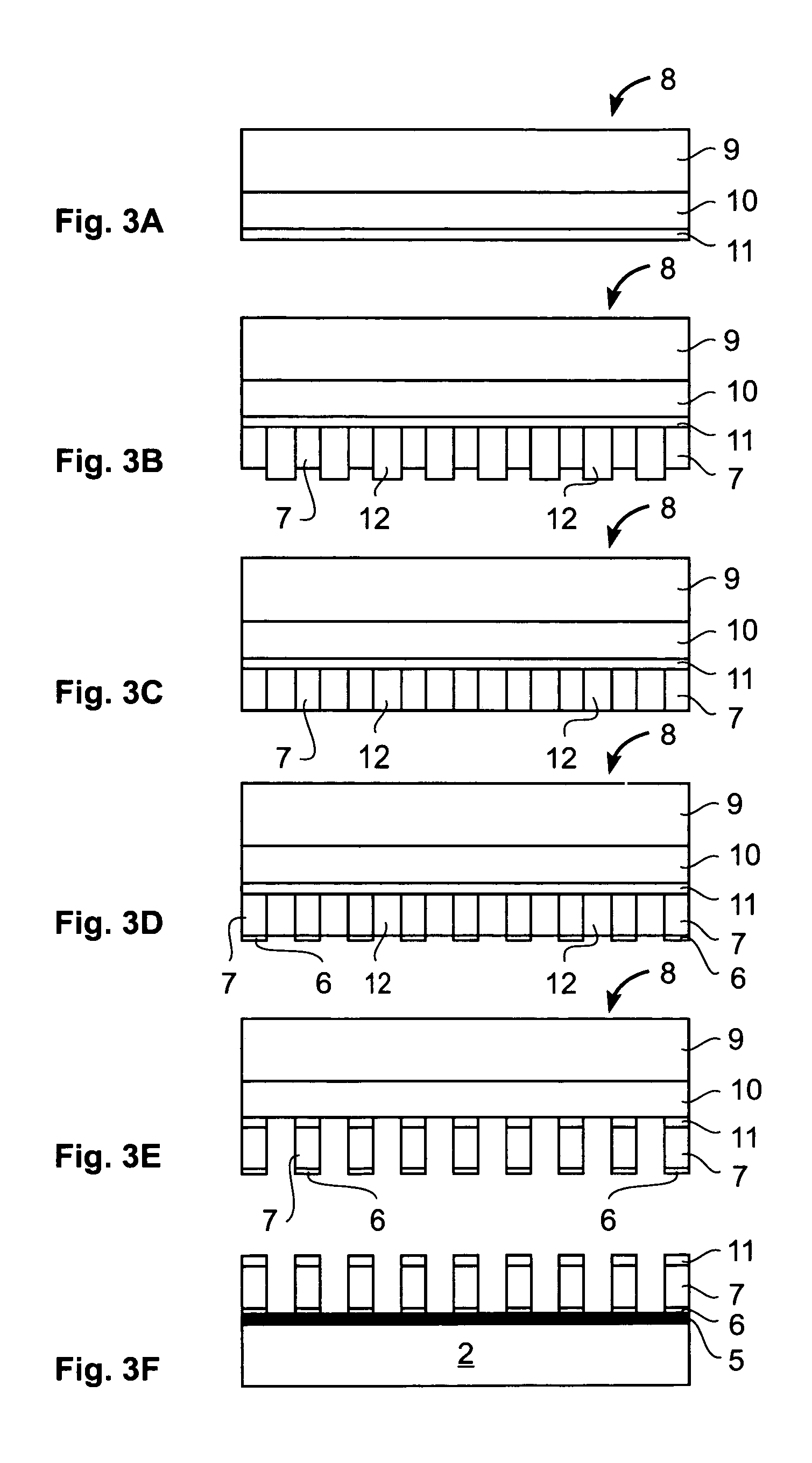
[0073]In order to produce a multi-chip module with a manifold layer, such as the multi-chip module 20 depicted in FIG. 4, the fabrication process described above with reference to FIGS. 3A to 3F can be utilized. After the steps of removing the carrier and mounting the semiconductor chips 2 onto a common substrate 3, a manifold layer is attached to the thermally conducting structure, i.e. a grid of connected fins or an array of frames, studs or fins, which is attached to the backsides of the semiconductor chips 2. Instead of fabricating a multi-chip module by using a carrier comprising a transparent substrate and a polyimide layer, as illustrated in FIGS. 3A to 3F, a manifold layer can be used as carrier, as well. For this, FIGS. 8A to 8H illustrate the fabrication process of a multi-chip module 40 according to the present invention.

[0074]In a first step, a manifold structure or manifold layer 41 having an electroconductive seed layer 11 is provided, as shown in FIG. 8A. Afterwards, ...


PUM


Abstract

Provides semiconductor devices and method for fabricating devices having a high thermal dissipation efficiency. An example device comprises a thermally conducting structure attached to a surface of the semiconductor device via soldering. The thermally conducting structure is essentially formed of a thermally conducting material and comprises an array of freestanding fins, studs or frames, or a grid of connected fins. A process for fabricating such a semiconductor device includes forming a thermally conducting structure on a carrier and attaching the thermally conducting structure formed on the carrier to a surface of the semiconductor device via soldering.

Description

FIELD OF THE INVENTION[0001]The present invention relates to a semiconductor device with a high thermal dissipation efficiency and to a method for fabricating the same.BACKGROUND[0002]In order to meet the demand for high clock frequencies of future computers, the integration density of current semiconductor devices as, for example, chips and multi-chip modules (MCM), in which a number of semiconductor chips are mounted on a common substrate generally in the face-down state, is continuously being increased. As a consequence, there arises the problem of increased heat dissipation due to the increase in power density.[0003]Common cooling approaches include air cooling, as for example disclosed in the U.S. Pat. No. 5,471,366, which describes a multi-chip module and a fabrication process thereof. The multi-chip module comprises a plurality of semiconductor chips mounted on a common substrate and a plurality of thermally conductive blocks attached to the semiconductor chips. A resin packa...

Claims


Application Information

Patent Timeline
Patent Type & Authority Patents(United States)
IPC IPC(8): H01L21/00H01L21/44H01L21/48H01L23/367
CPCH01L21/4871H01L21/4875H01L21/4882H01L23/3677H01L2924/1461H01L2224/16H01L2224/73253H01L2924/09701H01L2924/00
Inventor BRUNSCHWILER, THOMAS J.DESPONT, MICHELLANTZ, MARK A.MICHEL, BRUNOVETTIGER, PETER
Owner GLOBALFOUNDRIES US INC
Why Eureka
Try Eureka