Nitride semiconductor device
- Summary
- Abstract
- Description
- Claims
- Application Information
AI Technical Summary
Benefits of technology
Problems solved by technology
Method used
Image

Examples
first embodiment
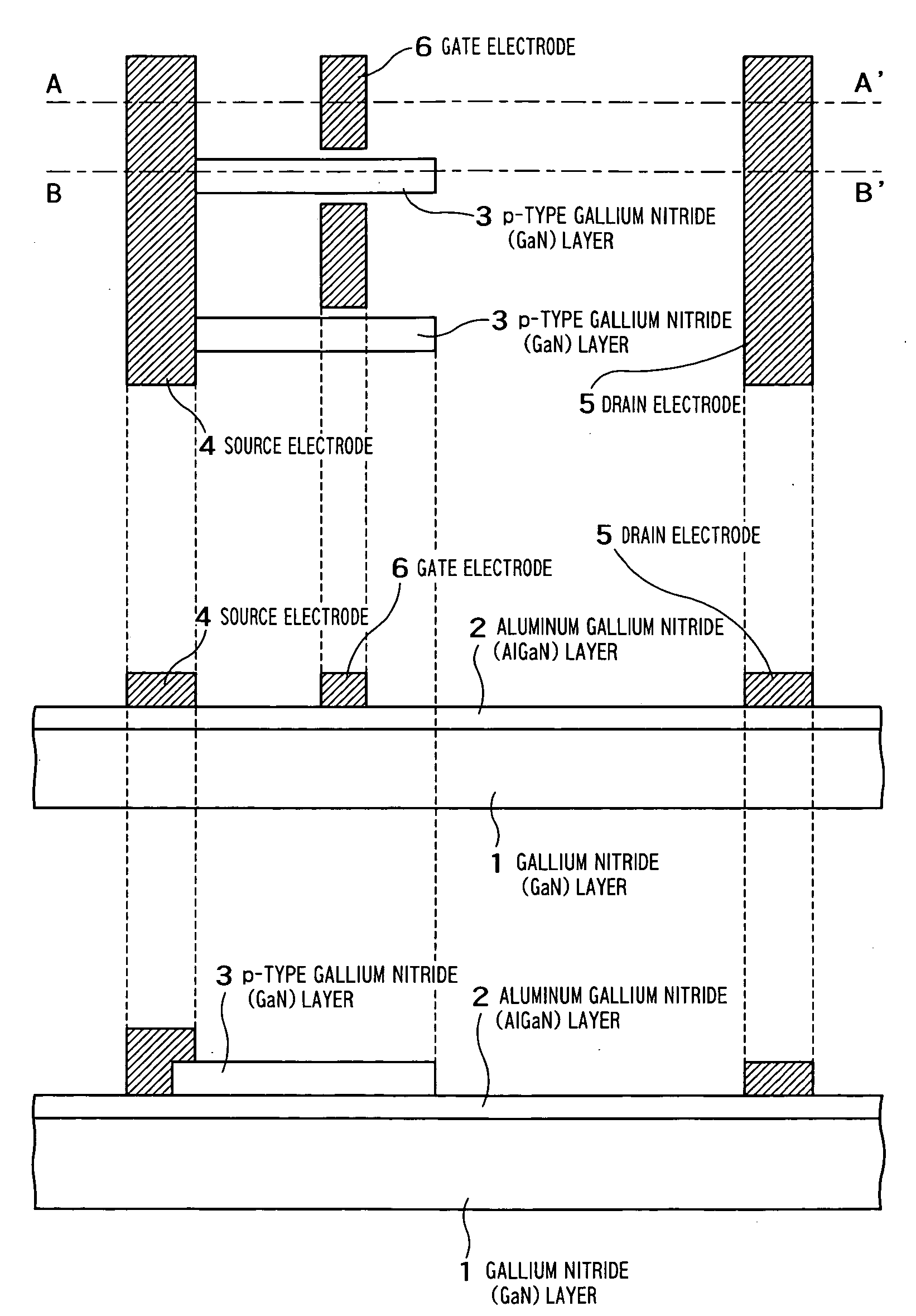
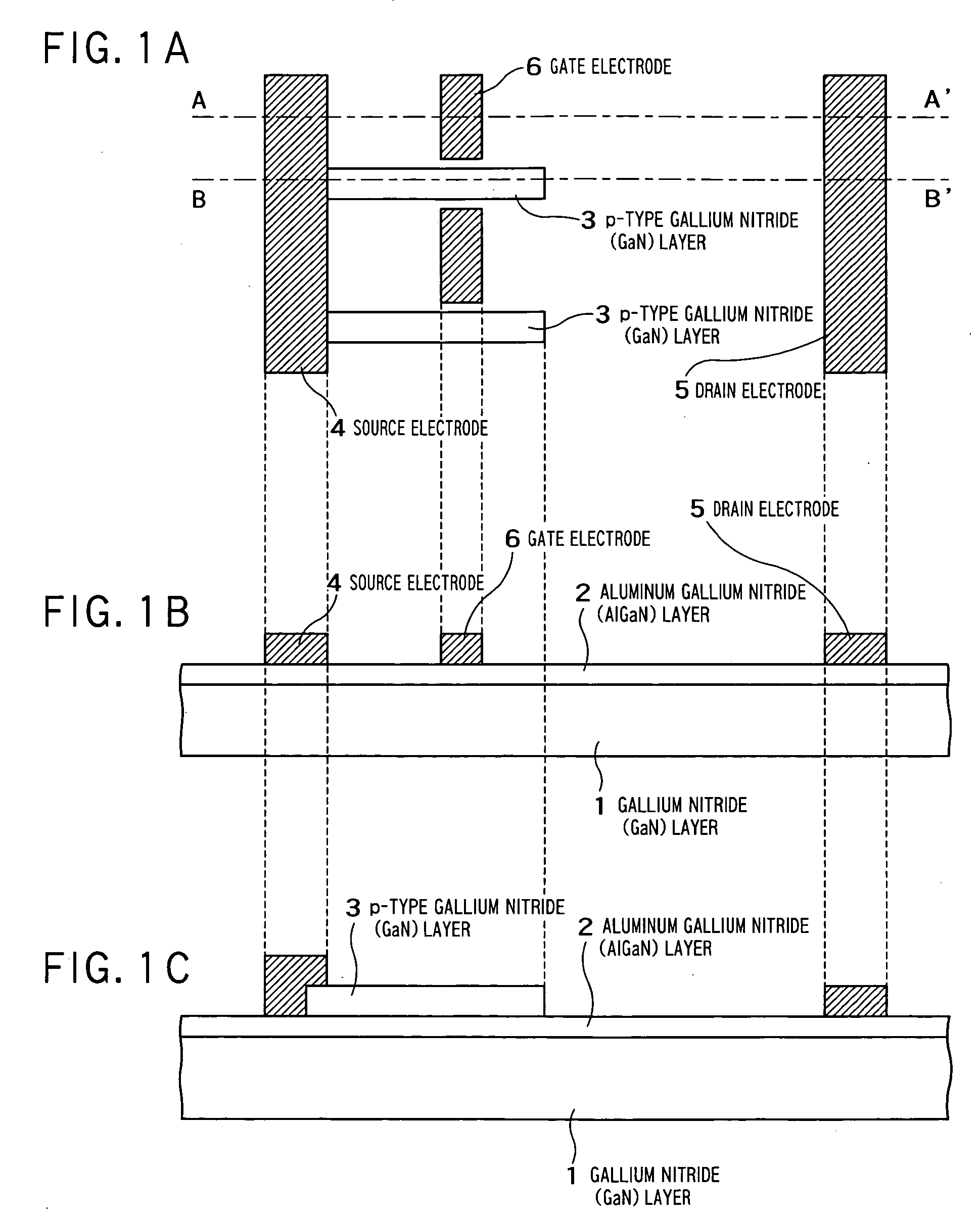
[0045]FIG. 1A is a plan view typically showing the configuration of a nitride power semiconductor device according to the present invention. FIGS. 1B and 1C are sectional views typically showing the configuration of the same. FIGS. 1B and 1C show sectional structures along lines A-A′ and B-B′ shown in FIG. 1A, respectively.
[0046]The nitride power semiconductor device according to the first embodiment of the present invention includes a undoped gallium nitride (GaN) layer 1 formed as a channel layer, an n-type aluminum gallium nitride (AlGaN) layer 2 formed as a barrier layer on the gallium nitride (GaN) layer 1, stripe-shaped p-type gallium nitride (GaN) layers 3 formed in substantially parallel to each other at predetermined intervals in a predetermined region on the n-type aluminum gallium nitride (AlGaN) layer 2, a source electrode 4 formed on the n-type aluminum gallium nitride (AlGaN) layer 2 to be electrically connected to one ends of the p-type gallium nitride (GaN) layers 3,...
second embodiment
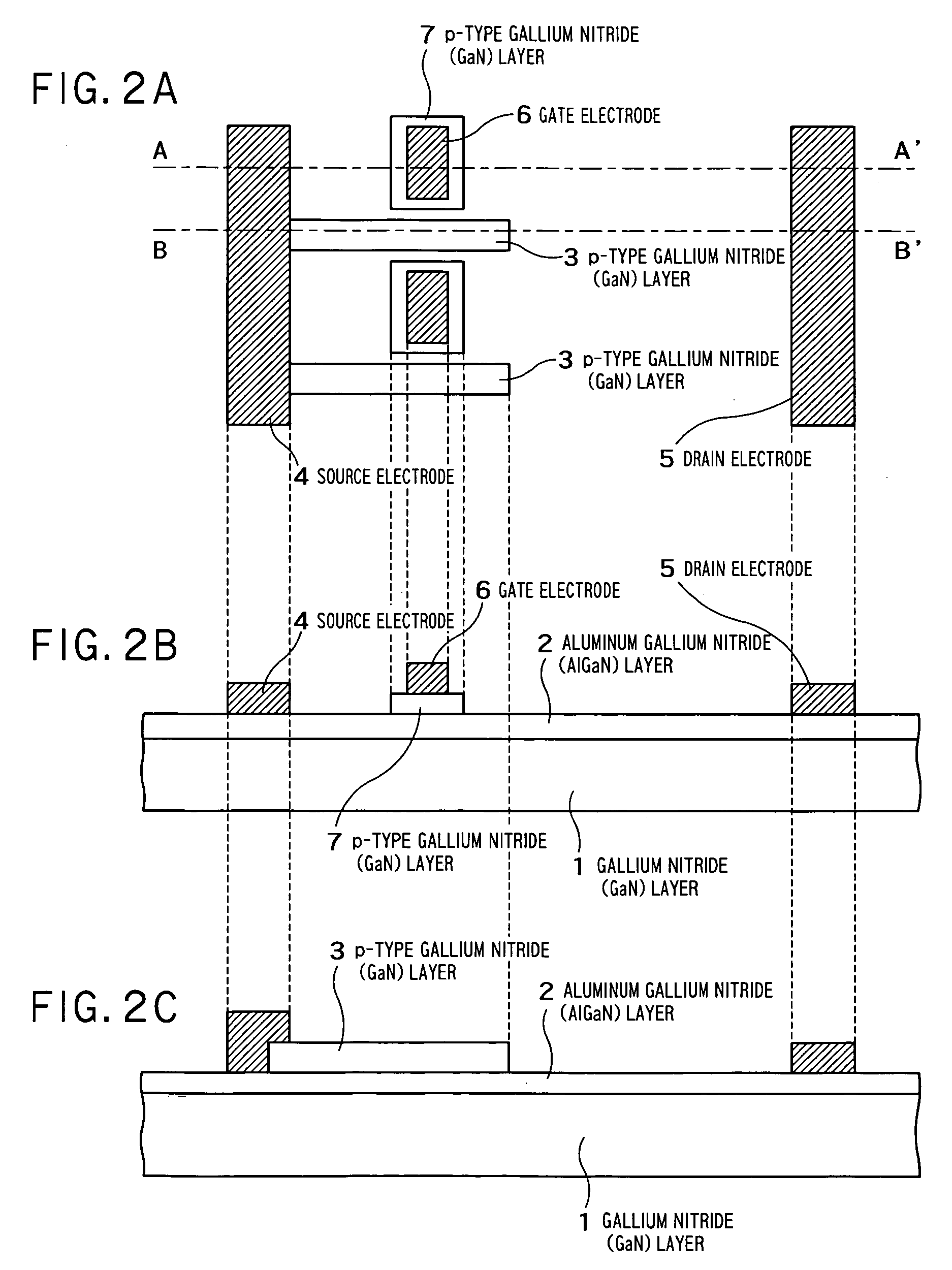
[0056]FIG. 2A is a plan view typically showing the configuration of a nitride power semiconductor device according to the present invention. FIGS. 2B and 2C are sectional views typically showing the configuration of the same. FIGS. 2B and 2C show sectional structures along lines A-A′ and B-B′ shown in FIG. 2A, respectively.
[0057]The nitride power semiconductor device according to the second embodiment of the present invention includes a undoped gallium nitride (GaN) layer 1 formed as a channel layer, an n-type aluminum gallium nitride (AlGaN) layer 2 formed as a barrier layer on the gallium nitride (GaN) layer 1, stripe-shaped p-type gallium nitride (GaN) layers 3 formed in substantially parallel to each other at predetermined intervals in a predetermined region on the n-type aluminum gallium nitride (AlGaN) layer 2, a source electrode 4 formed on the n-type aluminum gallium nitride (AlGaN) layer 2 to be electrically connected to one ends of the p-type gallium nitride (GaN) layers 3...
third embodiment
[0066]FIG. 4A is a plan view typically showing the configuration of a nitride power semiconductor device according to the present invention. FIGS. 4B and 4C are sectional views typically showing the configuration of the same. FIGS. 4B and 4C show sectional structures along lines A-A′ and B-B′ shown in FIG. 4A, respectively.
[0067]The nitride power semiconductor device according to the third embodiment of the present invention includes a undoped gallium nitride (GaN) layer 1 formed as a channel layer, an n-type aluminum gallium nitride (AlGaN) layer 2 formed as a barrier layer on the gallium nitride (GaN) layer 1, stripe-shaped p-type gallium nitride (GaN) layers 3 formed in substantially parallel to each other at predetermined intervals in a predetermined region on the n-type aluminum gallium nitride (AlGaN) layer 2, a source electrode 4 formed on the n-type aluminum gallium nitride (AlGaN) layer 2 to be electrically connected to one ends of the p-type gallium nitride (GaN) layers 3,...
PUM
 Abstract
Description
Claims
Application Information
 - R&D
- Intellectual Property
- Life Sciences
- Materials
- Tech Scout
- Unparalleled Data Quality
- Higher Quality Content
- 60% Fewer Hallucinations
Browse by: Latest US Patents, China's latest patents, Technical Efficacy Thesaurus, Application Domain, Technology Topic, Popular Technical Reports.
© 2025 PatSnap. All rights reserved.Legal|Privacy policy|Modern Slavery Act Transparency Statement|Sitemap|About US| Contact US: help@patsnap.com