

Inverted organic light emitting diode with doped layers
a light-emitting diode and organic technology, applied in the direction of discharge tube/lamp details, organic semiconductor devices, discharge tubes luminescnet screens, etc., can solve the problems of inability to meet the requirements of electron injection, etc., to achieve enhanced light emission efficiency and reduce operating voltage
- Summary
- Abstract
- Description
- Claims
- Application Information
AI Technical Summary
Benefits of technology
Problems solved by technology
Method used
Image

Examples
Embodiment Construction
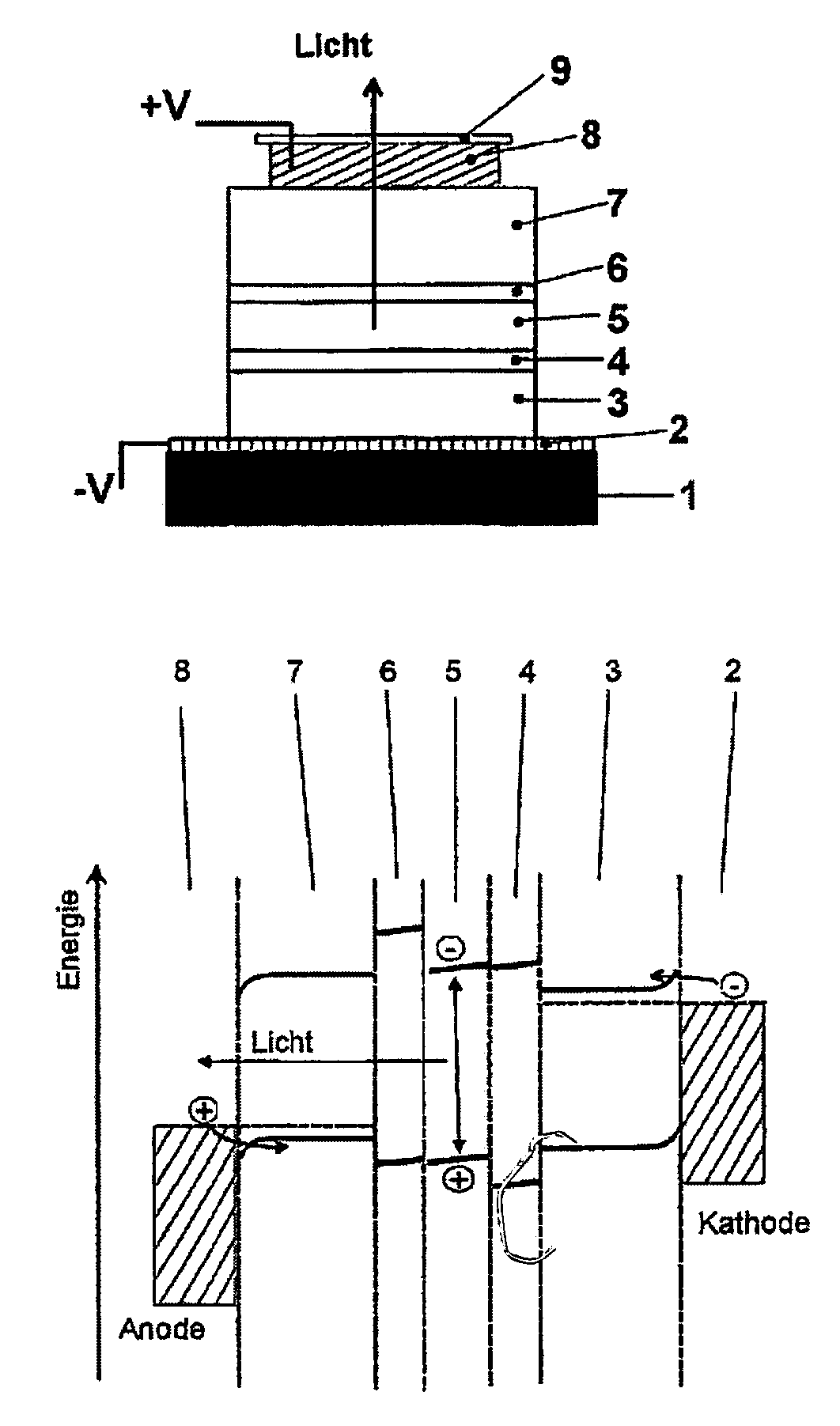
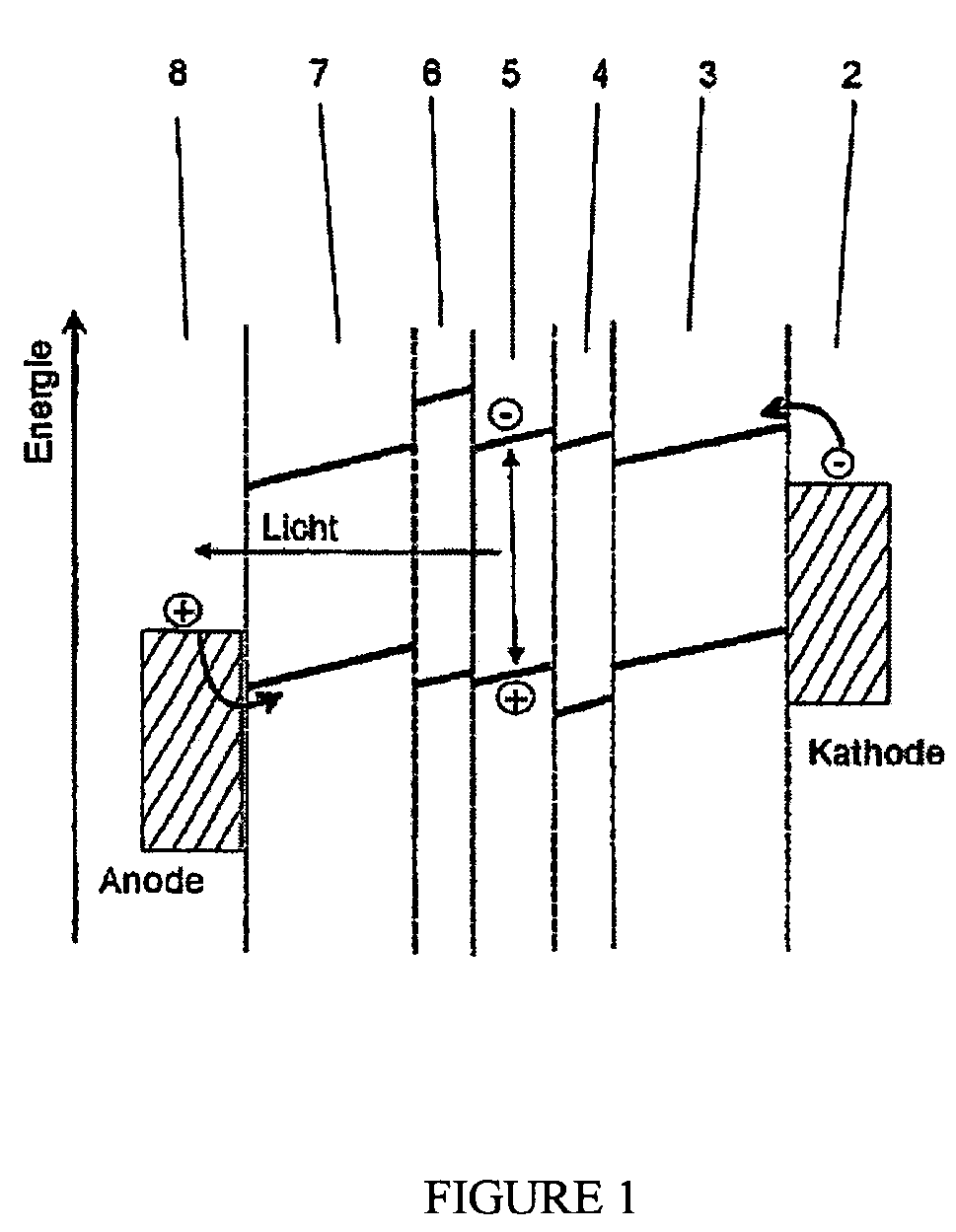
[0041]In the embodiment shown in FIG. 1, no space charge zone occurs at the hole-injecting contact. This embodiment calls for a low energy barrier for hole injection. Sometimes, this may not be achieved with available materials. Hence the injection of holes from the anode is less effective than for the conventional structure, where the work-function of the anode can be modified. Thus, the OLED exhibits an elevated operating voltage.
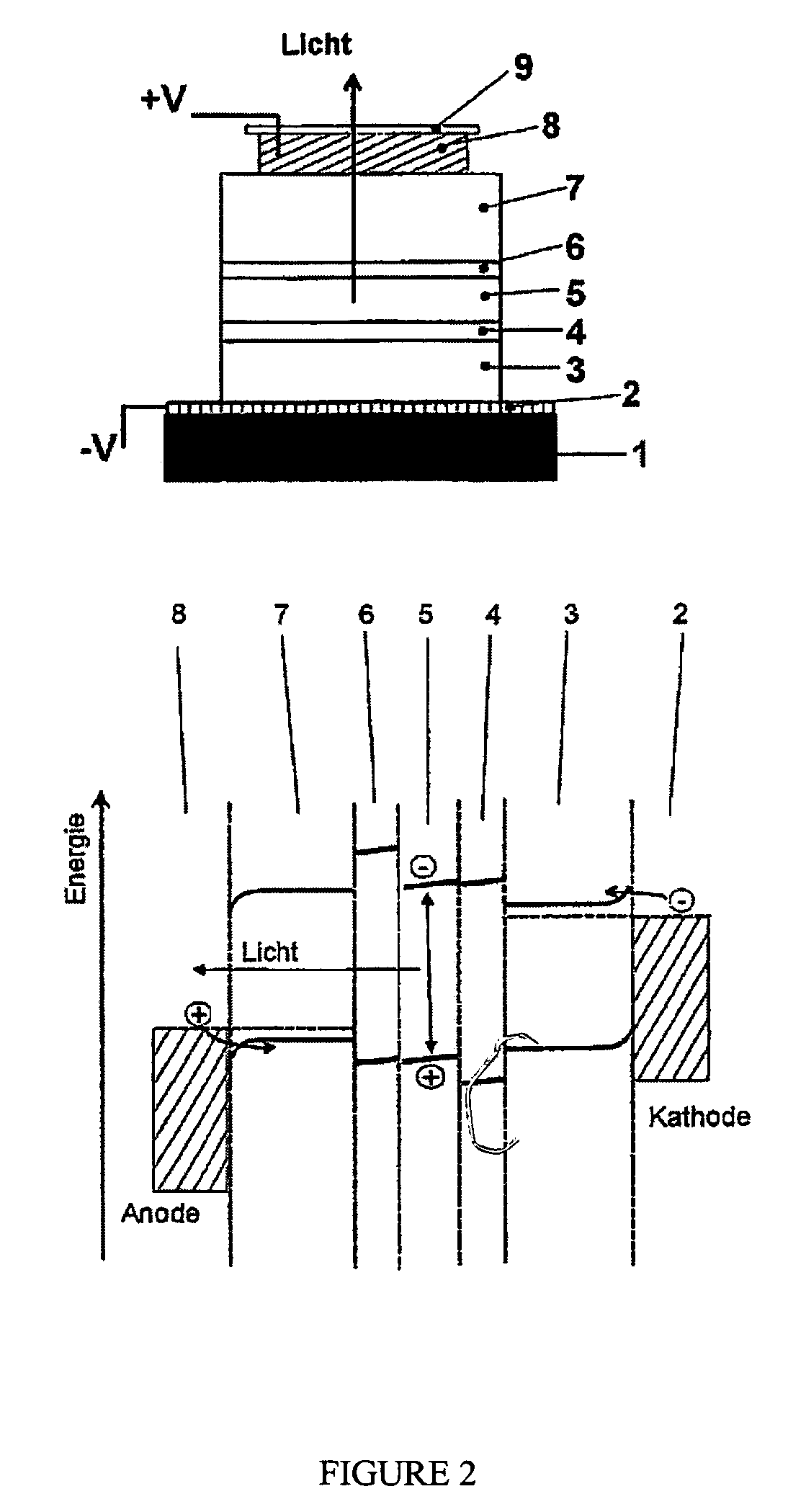
[0042]According to the invention, the disadvantage of prior structures is avoided by inverted OLEDs with doped injecting and transporting layers, optionally in combination with block layers 4, 6. FIG. 2 shows an exemplary apparatus in which the hole-injecting and -conducting layer 7 is doped, so that the boundary layer to the contact (anode 8) constitutes a space charge zone. The doping is high enough so that this space charge zone can be easily tunneled through. That such dopings are possible has already been shown in the literature for non-inverted ligh...
PUM
 Abstract
Description
Claims
Application Information