
Driver circuit and shift register of display device and display device

a shift register and drive circuit technology, applied in the direction of digital storage, instruments, turf growing, etc., can solve the problems of degrading display quality, reducing display uniformity, and keeping the circuit scale of the shift register small, so as to prevent the fluctuation of a signal supplied, small driving ability, and small circuit scale

Inactive Publication Date: 2007-09-25
SHARP KK
View PDF11 Cites 25 Cited by
  • Summary
  • Abstract
  • Description
  • Claims
  • Application Information

AI Technical Summary

Benefits of technology

[0012]The present invention is made in view of the foregoing conventional problems, and an object is to provide a driver circuit for a display device having an internal pre-charging circuit and carries out pre-charging of signal supplying lines with a pre-charging power source having small driving ability, and capable of preventing fluctuation of a signal supplied to other signal supplying lines while keeping the circuit scale of the shift register small. Further, the present invention also provides a shift register used for the driver circuit, and a display device including the driver circuit.
[0015]Accordingly, for performing pre-charging of signal supplying lines with an internal pre-charging circuit by using a pre-charging power source having small driving ability, the foregoing configuration can provide a driver circuit of a display device capable of preventing fluctuation of a signal supplied to a different signal supplying line, while keeping the circuit scale of the shift register small.
[0021]Therefore, in case of performing pre-charging of a signal supplying line with an internal pre-charging circuit by using a pre-charging power source having small driving ability, the foregoing arrangement can provide a shift register having a small circuit scale and is suitably used for a driver circuit for a display device capable of preventing fluctuation of a signal supplied to a different signal supplying line.
[0023]Therefore, when a data signal line driver performs pre-charging of a signal supplying line with an internal pre-charging circuit by using a pre-charging power source having small driving ability, the foregoing configuration can provide a driver circuit of a display device capable of preventing fluctuation of a signal supplied to a different signal supplying line, while keeping the circuit scale of the shift register small. As a result, display uniformity is ensured in the display device, thus providing a display device having high display quality.

Problems solved by technology

Such fluctuation of the video signal causes such as a decrease of display uniformity, thereby degrading display quality.
As has been explained, in case of carrying out pre-charging of a signal supplying line, such as a data signal line, with an internal pre-charging circuit by using a pre-charging power source having small driving ability, a conventional driver circuit of a display device such as a data signal line driver has failed to prevent fluctuation of a signal supplied to other signal supplying line while keeping the circuit scale of the shift register small.

Method used


Image

  • Driver circuit and shift register of display device and display device
  • Driver circuit and shift register of display device and display device
  • Driver circuit and shift register of display device and display device

Examples


first embodiment

[0044]The following will explain one embodiment of the present invention with reference to FIGS. 1 and 2.

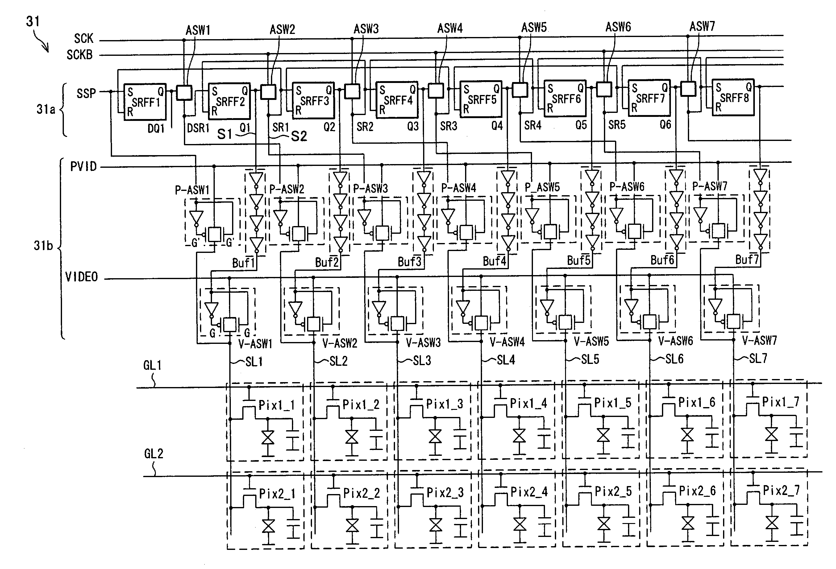
[0045]The present embodiment uses a data signal line driver included in a liquid crystal display device, as a driver circuit of a display device of the present invention. FIG. 1 shows a configuration of a data signal line driver 31 as an example of such a data signal line driver.

[0046]The data signal line driver 31 includes a shift register 31a and a sampling section 31b.

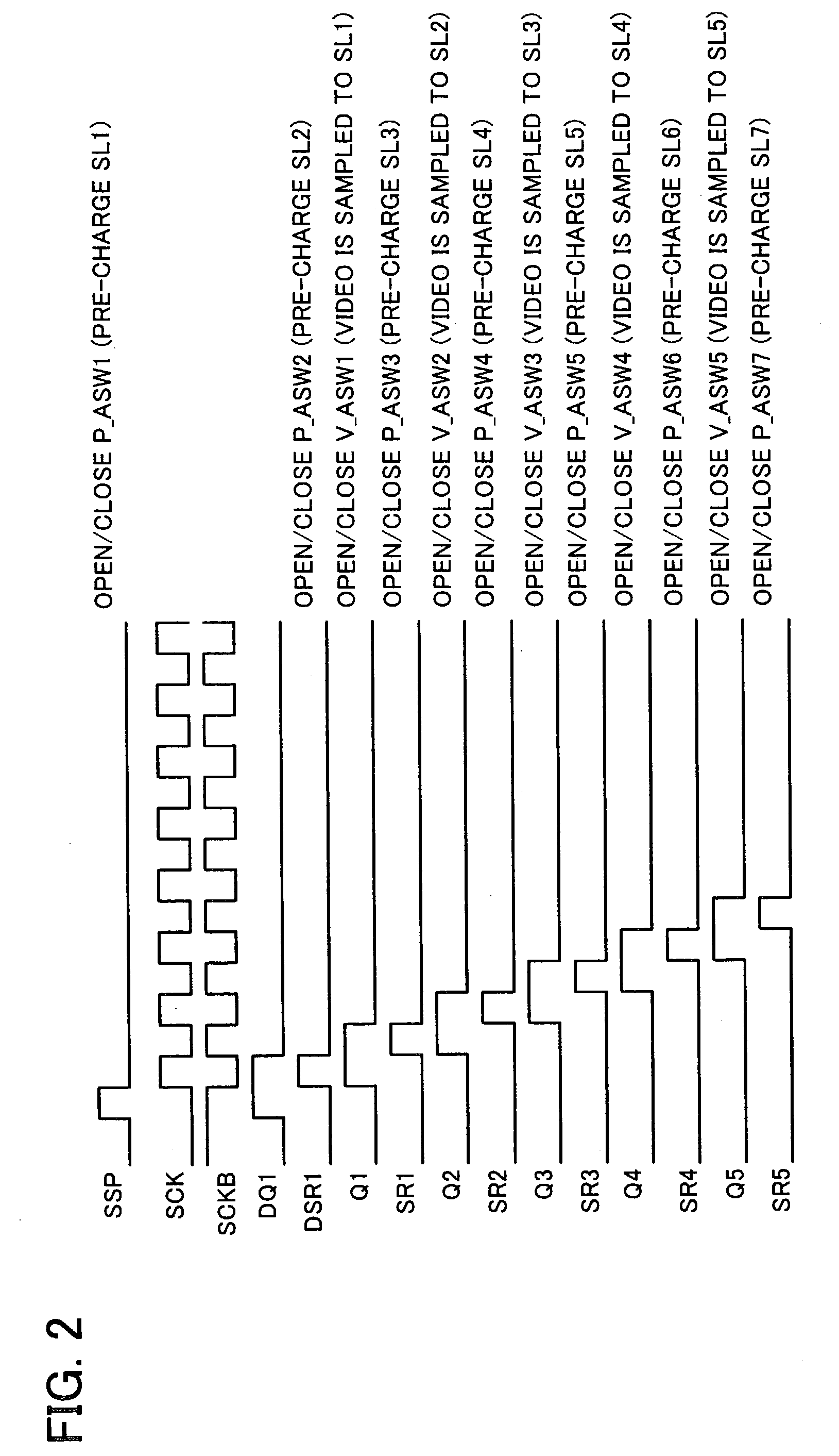
[0047]The shift register 31a includes plural stages of set-reset type flip-flops SRFF1, SRFF2, . . . , and plural switch circuits (control signal supplying circuit) ASW1, ASW2, . . . The switch circuit ASWk (k=1, 2, . . . ) uses a Q output of the flip-flop SRFFk as a control signal for switching itself between a conductive state and a non-conductive state. Upon its conductive state, an odd-numbered switch circuit ASWk receives a clock signal (pre-charging control signal (a signal for carrying out pre-charging)) ...

second embodiment

[0066]The following will explain another embodiment of the present invention with reference to FIGS. 3 and 4. For ease of explanation, materials having the equivalent functions as those shown in the drawings pertaining to First Embodiment above will be given the same reference symbols, and explanation thereof will be omitted here.

[0067]The present embodiment uses a data signal line driver included in a liquid crystal display device, as a driver circuit of a display device of the present invention. FIG. 3 shows a configuration of a data signal line driver 32 as an example of such a data signal line driver.

[0068]The data signal line driver 32 includes a shift register 32a and a sampling section (writing circuit, pre-charging circuit) 32b.

[0069]The shift register 32a has the same internal arrangement as that of the shift register 31a; however, in this shift register 32a, the signal for pre-charging is outputted to a different switch. The start pulse SSP used as a set signal of the fli...

third embodiment

[0073]The following will explain a still another embodiment of the present invention with reference to FIGS. 5 and 6. For ease of explanation, materials having the equivalent functions as those shown in the drawings pertaining to First and Second Embodiments above will be given the same reference symbols, and explanation thereof will be omitted here.

[0074]The present embodiment uses a data signal line driver included in a liquid crystal display device, as a driver circuit of a display device of the present invention. FIG. 5 shows a configuration of a data signal line driver 33 as an example of such a data signal line driver.

[0075]The data signal line driver 33 includes a shift register 33a and a sampling section (writing circuit, pre-charging circuit) 33b.

[0076]The shift register 33a includes plural stages of D flip-flop: flip-flops DFFD1, DFF1, DFF2, . . . , and plural switch circuits ASWD1, ASW1, ASW2, . . . An input signal IN of the first stage flip flop DFFD1 is the start pulse...


PUM


Abstract

A driver circuit for a display device includes a plurality of set-reset flip-flops and switch circuits, and is arranged so that a timing pulse for sampling outputted from the flip-flop is supplied to the switch circuit, so as to cause the switch circuit to receive a clock signal. The clock signal operates as a set signal of the next stage flip-flop and outputted as a control signal for carrying out pre-charging of a data signal line and a selected pixel connected to the data signal line, with a switch. Thus, in case of performing pre-charging of a signal supplying line with an internal pre-charging circuit by using a pre-charging power source having small driving ability, this arrangement can provide a driver circuit for a display device capable of preventing fluctuation of a signal supplied to a different signal supplying line, while keeping the circuit scale of the shift register small.

Description

FIELD OF THE INVENTION[0001]The present invention relates to a driver circuit for carrying out pre-charging and supplying a signal with respect to signal supplying lines of a display device, and also relates to a shift register, and a display device.BACKGROUND OF THE INVENTION[0002]When a liquid crystal panel is driven by alternating driving in an active matrix type liquid crystal display device adopting a point-at-a-time method, a data signal line is pre-charged before a pixel is supplied with a video signal via the data signal line, so that each pixel is stably charged to a predetermined charge amount. In this arrangement, when the pre-charging is carried out with respect to all data signal lines at the same time, the power source for pre-charging is required to have high driving ability so as to deal with large writing amount for all data signal lines. Some pre-charging systems have been introduced as technologies to solve this problem by carrying out pre-charging with respect to...

Claims


Application Information

Patent Timeline
IPC IPC(8): G09G3/36G02F1/133G09G3/20G11C19/00
CPCG09G3/3688G09G2310/0248A01G20/00A01G9/029
Inventor WASHIO, HAJIMEHAYASHI, SHUNSUKE
Owner SHARP KK
Features
  • Generate Ideas
  • Intellectual Property
  • Life Sciences
  • Materials
  • Tech Scout
  • Unparalleled Data Quality
  • Higher Quality Content
  • 60% Fewer Hallucinations
Learn More