Edge illuminated photodiodes

a photodiode and edge illumination technology, applied in the field of photodiodes, can solve the problems of low responsivity due to edge surface recombination, the difficulty of controlling quantum efficiency, and the current photodiode, so as to improve the operational and structural characteristics

Inactive Publication Date: 2007-10-09
OSI OPTOELECTRONICS
View PDF37 Cites 56 Cited by
  • Summary
  • Abstract
  • Description
  • Claims
  • Application Information

AI Technical Summary

Benefits of technology

[0009]The present invention is directed toward photodiodes having improved operational and structural characteristics. In one embodiment, the present invention is a photodiode comprising a substrate with at least a plurality of facets, wherein said plurality of facets comprise a proximate facet substantially comprising a region doped with an impurity of a first conductivity type; a distant facet parallel to the proximate facet; a top facet having an anode metallization region and having a region proximate to said anode metallization region doped with an impurity of a second conductivity type; a bottom facet having a cathode metallization layer; a left facet; and a right facet parallel to the left facet.

Problems solved by technology

Several problems exist with conventional photodiodes currently in use.
In particular, for relatively short wavelength illumination, for instance below 800 nm, edge-illuminated silicon photodiodes absorb light very strongly near the edge surfaces thereby leading to low responsivity due to edge surface recombination.
Likewise, controlling quantum efficiency, specifically in case of edge illuminated InGaAs / InP photodiodes, still remains a challenge.
The prior art fails to describe edge illuminated photodiodes that provide for lesser susceptibility to surface recombination effects, and possess high responsivity, and high quantum efficiency respectively.

Method used


Image

  • Edge illuminated photodiodes
  • Edge illuminated photodiodes
  • Edge illuminated photodiodes

Examples


first embodiment

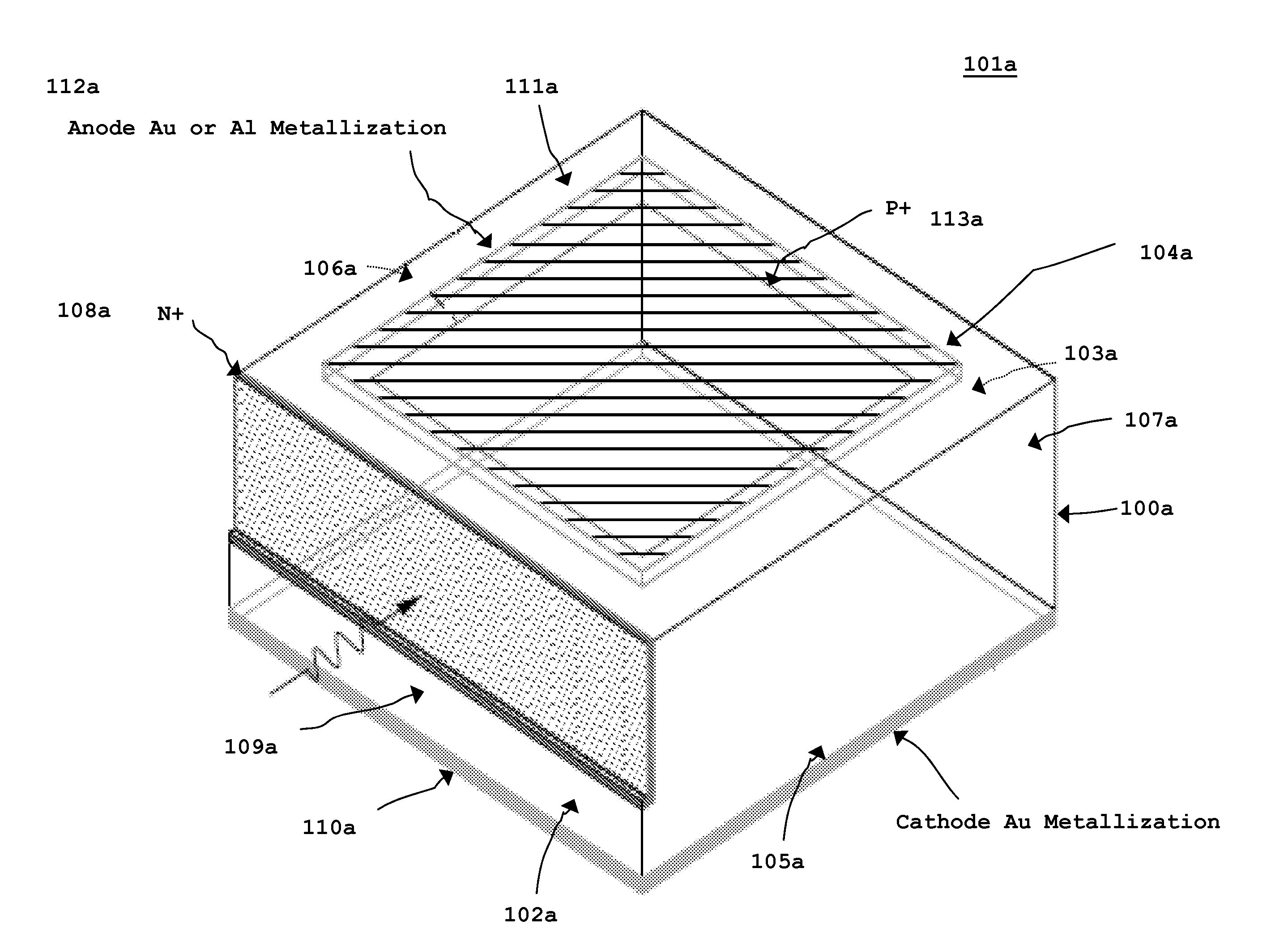
[0027]In a first embodiment, the edge illuminated photodiode is incorporated in a photochip having six distinct facets, namely proximate, distant, top, bottom, left, and right respectively. The proximate and distant facets are substantially parallel to each other. The top and bottom facets are substantially parallel to each other, and the left and right facets are substantially parallel to each other. The proximate facet substantially comprises an n+ diffused region. The bottom facet comprises a cathode metallization layer. The top facet comprises two regions, namely an anode metallization region and a p+ doped region. The p+ doped region is juxtaposed to the anode metallization region.

second embodiment

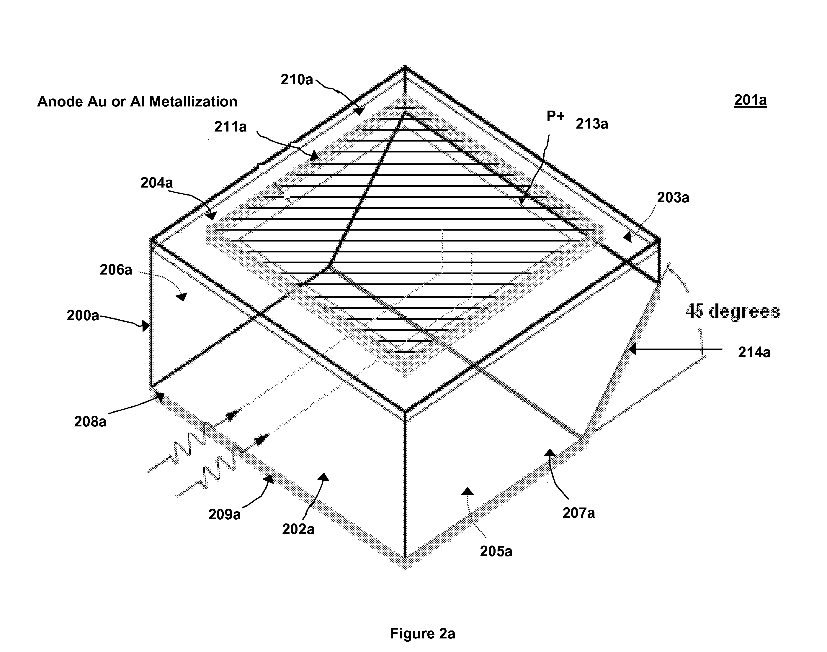
[0028]In second embodiment, an edge illuminated photodiode is incorporated in a substrate having seven distinct facets. Six facets include a proximate, distant, top, bottom, left, and right facet, respectively. The proximate and distant facets are substantially parallel to each other. The top and bottom facets are substantially parallel to each other, and the left and right facets are substantially parallel to each other. The seventh facet is formed at an angle to no less than two facets, i.e., the distant and bottom facets, respectively. Preferably the angle of formation, measured relative to the internal face of each facet (the sides facing the inside of the photodiode), is greater than 90 degrees. More preferably, the angle of formation is 135 degrees.

[0029]In one embodiment, the top facet comprises two regions, namely an anode metallization region and a p+ doped and textured region. The p+ region, juxtaposed to the anode metallization region, is textured to reduce reflectance at...

third embodiment

[0049]an edge illuminated photodiode of the present invention is depicted in FIG. 2c. Photodiode 201c comprises photochip 200c, which is made of a suitable semiconductor material possessing apt geometrical specifications. For example, and by no way of limitation, photochip 200c comprises silicon that is cuboidal in geometry. The cuboid (or rectangular parallelepiped) shaped photochip 200c has six distinct facets. For purposes of elucidation, the sides or facets of photochip 200c have been enumerated as proximate 202c, distant 203c, top 204c, bottom 205c, left 206c, and right 207c. Persons of ordinary skill would appreciate that the present designation of photochip geometry is not limited to the description provided herein and can be adjusted to suit other design, fabrication, and functional specifications.

[0050]Bottom surface 205a is subjected to metallization in accordance with the principles of the present invention. Consequently, bottom facet 205a comprises a finish layer 220c. F...


PUM


Abstract

This invention comprises plurality of edge illuminated photodiodes. More specifically, the photodiodes of the present invention comprise novel structures designed to minimize reductions in responsivity due to edge surface recombination and improve quantum efficiency. The novel structures include, but are not limited to, angled facets, textured surface regions, and appropriately doped edge regions.

Description

FIELD OF THE INVENTION[0001]The present invention is directed toward photodiodes having improved operational and structural characteristics. More specifically, the present invention is directed towards novel edge illuminated photodiodes, and applications using the same, possessing high responsivity, enhanced quantum efficiency using n+ diffused region, and p+ textured region on silicon, and InGaAs / InP substrates respectively.BACKGROUND OF THE INVENTION[0002]Photodiodes comprise a plurality of electrode radiation-sensitive junctions formed in semiconductor material. Within a photodiode, charge carriers are created by light that illuminates the junction and photo current is generated dependent upon the degree of illumination. Photodiodes are used for detection of optical power and subsequent conversion of the same to electrical power. Operationally, photodiodes absorb photons and charged particles, which facilitate detection of incident optical power, thereby generating current propor...

Claims


Application Information

Patent Timeline
Patent Type & Authority Patents(United States)
IPC IPC(8): H01L31/062H01L31/0232H01L31/06H01L31/113
CPCH01L31/0236H01L31/035281H01L31/102H01L31/028Y02E10/50H01L31/0304H01L31/02363
Inventor BUI, PETER STEVENTANEJA, NARAYAN DASSMANSOURI, MANOOCHER
Owner OSI OPTOELECTRONICS
Why Eureka
Try Eureka