Power LDMOS transistor

a technology of mos transistor and power ldmos, which is applied in the direction of semiconductor/solid-state device manufacturing, semiconductor devices, electrical apparatus, etc., can solve the problems of limiting the current handling capability of the transistor, challenging and often times more expensive design of the mos transistor, and not being able to meet the needs of power management applications

Active Publication Date: 2007-10-16
CICLON SEMICON DEVICE
View PDF23 Cites 118 Cited by
  • Summary
  • Abstract
  • Description
  • Claims
  • Application Information

AI Technical Summary

Problems solved by technology

When used in PWM applications, the transistors must exhibit small power loss during switching, which imposes an additional requirement—small internal capacitances—that make the MOSFET design challenging and often times more expensive.
The thick epitaxial layer and P+ substrate result in a high on resistance (Rds,on) of the device, which is not acceptable for power management applications.
This in turn leads to a de-biasing effect known for lateral devices (voltage drop along a stripe electrode under high current conditions) and limits the current handling capability of the transistor.

Method used


Image

  • Power LDMOS transistor
  • Power LDMOS transistor
  • Power LDMOS transistor

Examples


Embodiment Construction

[0014]As used herein, the following dopant concentrations are distinguished using the following notations:[0015](a) N++ or P++: dopant concentration>5×10¹⁹ atoms / cm3;[0016](b) N+ or P+: dopant concentration of 1×10¹⁸ to 5×10¹⁹ atoms / cm3;[0017](c) N or P: dopant concentration of 5×10¹⁶ to 1×10¹⁸ atoms / cm3;[0018](d) N− or P−: dopant concentration of 1×10¹⁵ to 5×10¹⁶ atoms / cm3;[0019](e) N−− or P−−: dopant concentration15 atoms / cm3.

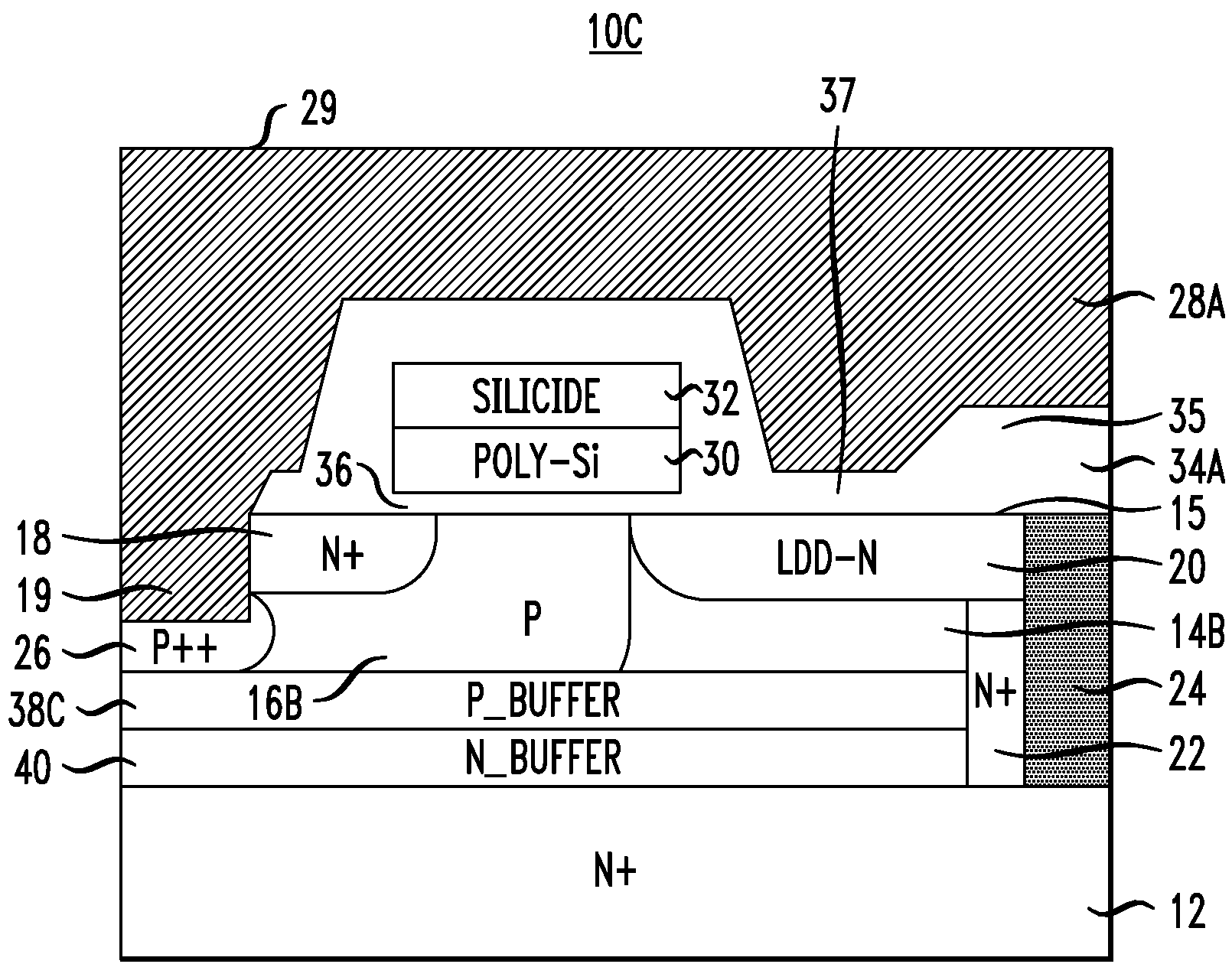
[0020]FIG. 1 is an illustration of an embodiment of an improved power transistor, more specifically and improved LDMOS transistor 10. In exemplary applications, the transistor 10 is used as a switch in a voltage regulator of a power supply for, for example, a server or desktop computer or in a DC / DC converter for general use.

[0021]Specifically, FIG. 1 illustrates an improved n-channel LDMOS device. The transistor structure 10 includes a semiconductor substrate 12, which, in the illustrated embodiment, is preferably a highly doped (N+) silicon wafer doped with...


PUM


Abstract

An LDMOS device comprises a substrate having a first conductivity type and a lightly doped epitaxial layer thereon having an upper surface. Source and drain regions of the first conductivity type are formed in the epitaxial layer along with a channel region of a second conductivity type formed therebetween. A conductive gate is formed over a gate dielectric layer. A drain contact electrically connects the drain region to the substrate, comprising a first trench formed from the upper surface of the epitaxial layer to the substrate and having a side wall along the epitaxial layer, a highly doped region of the first conductivity type formed along the side wall of the first trench, and a drain plug in the first trench adjacent the highly doped region. A source contact is provided and an insulating layer is formed between the conductive gate and the source contact.

Description

FIELD OF THE INVENTION[0001]The present invention relates to semiconductor structures and more particularly to laterally diffused MOS transistors (LDMOS), and still more particularly to LDMOS transistors designed for low voltage power management applications.BACKGROUND OF THE INVENTION[0002]Power MOSFETs (metal oxide semiconductor (MOS) field effect transistors (FET)) are used as electric switches for high frequency PWM (pulse width modulation) applications such as voltage regulators and / or as load switches in power applications. When used as load switches, where switching times are usually long, cost, size and on-resistance of the switches are the prevailing design considerations. When used in PWM applications, the transistors must exhibit small power loss during switching, which imposes an additional requirement—small internal capacitances—that make the MOSFET design challenging and often times more expensive. Special attention has been paid to the Gate-to-Drain (Cgd) capacitance,...

Claims


Application Information

Patent Timeline
Patent Type & Authority Patents(United States)
IPC IPC(8): H01L29/76H01L29/94H01L31/00
CPCH01L29/41741H01L29/4175H01L29/7823H01L29/41766H01L29/7802H01L29/7811H01L29/7816H01L29/0634H01L29/0878H01L29/1095H01L29/402H01L29/4933H01L29/41758
Inventor XU, SHUMINGKOREC, JACEK
Owner CICLON SEMICON DEVICE
Why Eureka
Try Eureka