Electro-optical display having an arrangement of active and dummy coloring pixels performing as a color filter element
a color filter element and electrooptical display technology, applied in the direction of optical elements, instruments, address electrodes, etc., can solve the problems of reducing the ink volum
- Summary
- Abstract
- Description
- Claims
- Application Information
AI Technical Summary
Benefits of technology
Problems solved by technology
Method used
Image
Examples
first embodiment
[0036]1-1. First Embodiment
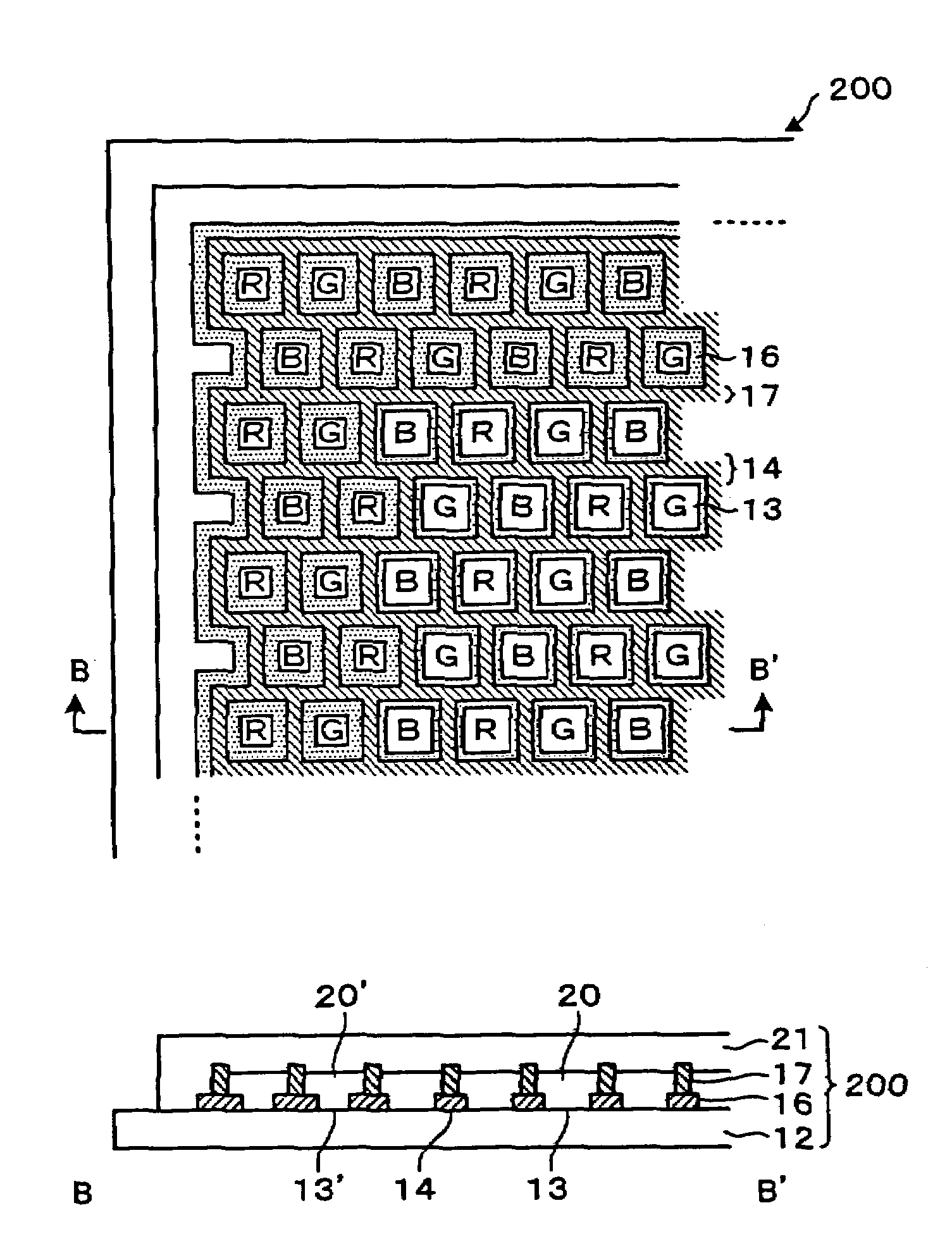
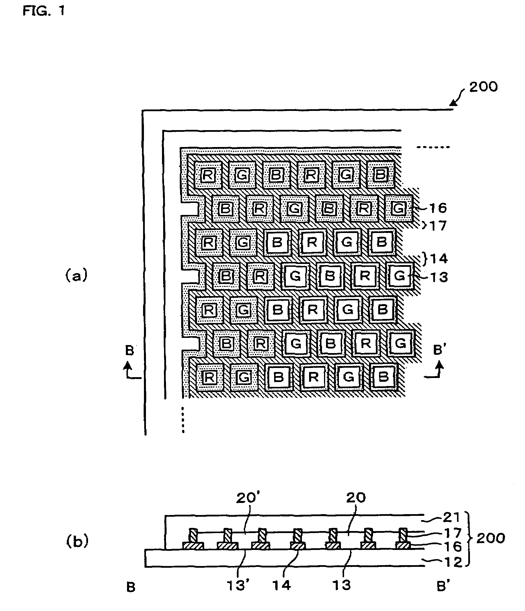
[0037]FIG. 1 is a partial enlarged view of a color filter of a first embodiment of this invention. FIG. 1(a) is a plan view, and FIG. 1(b) is a cross-sectional view along line B-B′ in FIG. 1(a).
[0038]As shown in FIG. 1(a), the color filter 200 comprises pixels 13 arranged in a matrix on the transparent substrate 12; the boundaries between the pixels are divided by partitions 14. Into each of the pixels 13 is introduced an ink in one of the colors red (R), green (G), and blue (B). In this example, the colors red, green, and blue are arranged in a so-called mosaic array. However, other arrangements, such as a stripe array or a delta array, may be used.
[0039]As shown in FIG. 1(b), the color filter 200 comprises a transparent substrate 12 and light-shielding partitions 14. The pixels 13 are formed in portions in which the partitions 14 are not formed (are removed). The inks of different colors introduced into the pixels 13 constitute the coloring layer 20. An ...
second embodiment
[0053]1-2. Second Embodiment
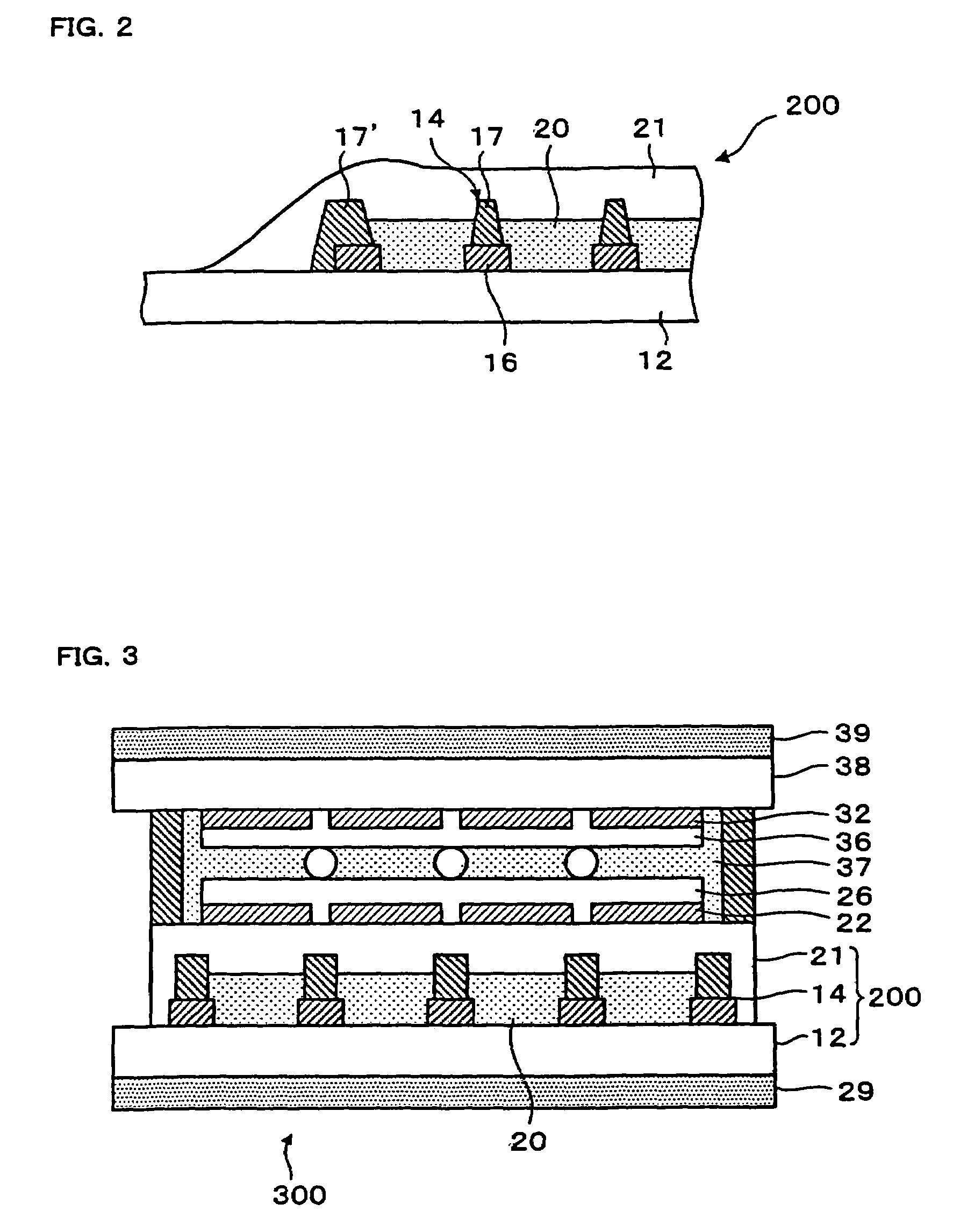
[0054]FIG. 2 is a partial cross-sectional view of a modification of the color filter of FIG. 1. This color filter comprises partitions 14; the partitions 14 are similar to those of the example of FIG. 1 in that a bank layer 17 is formed on top of a shielding layer 16, but the cross-sectional shape of the outermost portion 17′ of the bank layer 17 comprised by the partitions 14 differs from the example of FIG. 1.
[0055]In particular, the outermost portion 17′ of the bank layer 17 is formed with a greater width than the other portions of the bank layer 17, and has a portion extending outside the outermost portion of the shielding layer 16 and in direct contact with the substrate 12. As a result, the overcoat layer 21 and shielding layer 16 are isolated, and are in a state of mutual non-contact.
[0056]When forming the bank 17 of resin, because the outermost portion 17′ is formed with a greater width, the heat capacity of the outer portion can be increased. Hen...
PUM
| Property | Measurement | Unit |
|---|---|---|
| width | aaaaa | aaaaa |
| width | aaaaa | aaaaa |
| width | aaaaa | aaaaa |
Abstract
Description
Claims
Application Information
 - R&D
- Intellectual Property
- Life Sciences
- Materials
- Tech Scout
- Unparalleled Data Quality
- Higher Quality Content
- 60% Fewer Hallucinations
Browse by: Latest US Patents, China's latest patents, Technical Efficacy Thesaurus, Application Domain, Technology Topic, Popular Technical Reports.
© 2025 PatSnap. All rights reserved.Legal|Privacy policy|Modern Slavery Act Transparency Statement|Sitemap|About US| Contact US: help@patsnap.com


