Defect inspection method and defect inspection device

a defect detection and defect technology, applied in semiconductor/solid-state device testing/measurement, instruments, material analysis, etc., can solve the problems of defect detection sensitivity decreasing and detection sensitivity difficult to improve, and achieve high-sensitivity inspection

Active Publication Date: 2016-06-09
HITACHI HIGH-TECH CORP
View PDF6 Cites 2 Cited by
  • Summary
  • Abstract
  • Description
  • Claims
  • Application Information

AI Technical Summary

Benefits of technology

[0036]In accordance with the present invention, adoption of the configuration outlined above enables high-NA (numerical aperture) detection of images from

Problems solved by technology

During the inspection of a semiconductor wafer, in particular, the detection of even more microscopic defects is being demanded in response to the progress of further microstructured patterning, and how accurately a very weak defect signal from a microscopic defect can be extracted distinctively from background light noise is a big technological challenge associated with defect inspection.
One of the problems is how to augment a detection aperture (numerical aperture: NA) of the optical system to detect more efficiently the very weak light scattered from microscopic defects.

Method used


Image

  • Defect inspection method and defect inspection device
  • Defect inspection method and defect inspection device
  • Defect inspection method and defect inspection device

Examples


first embodiment

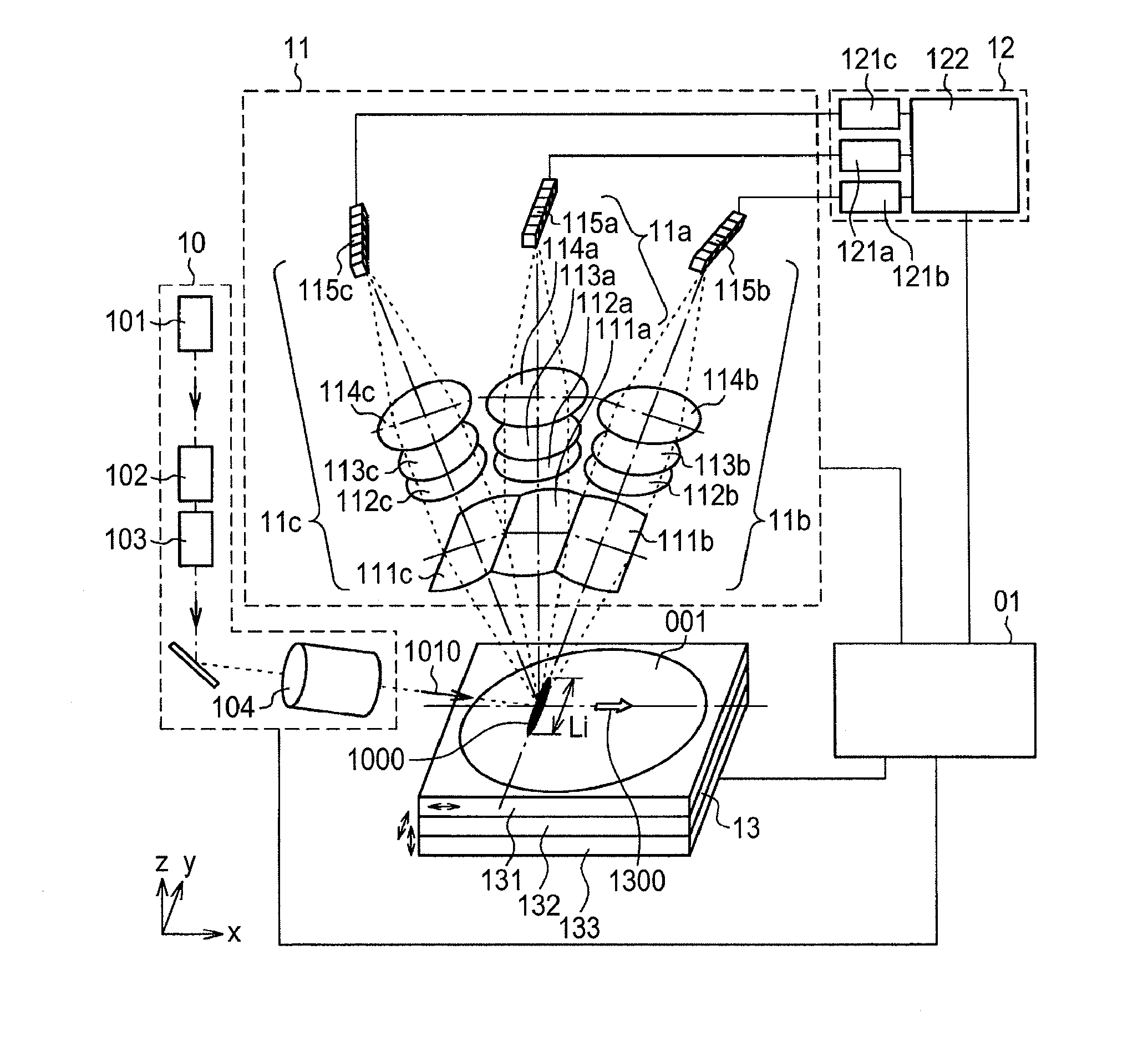
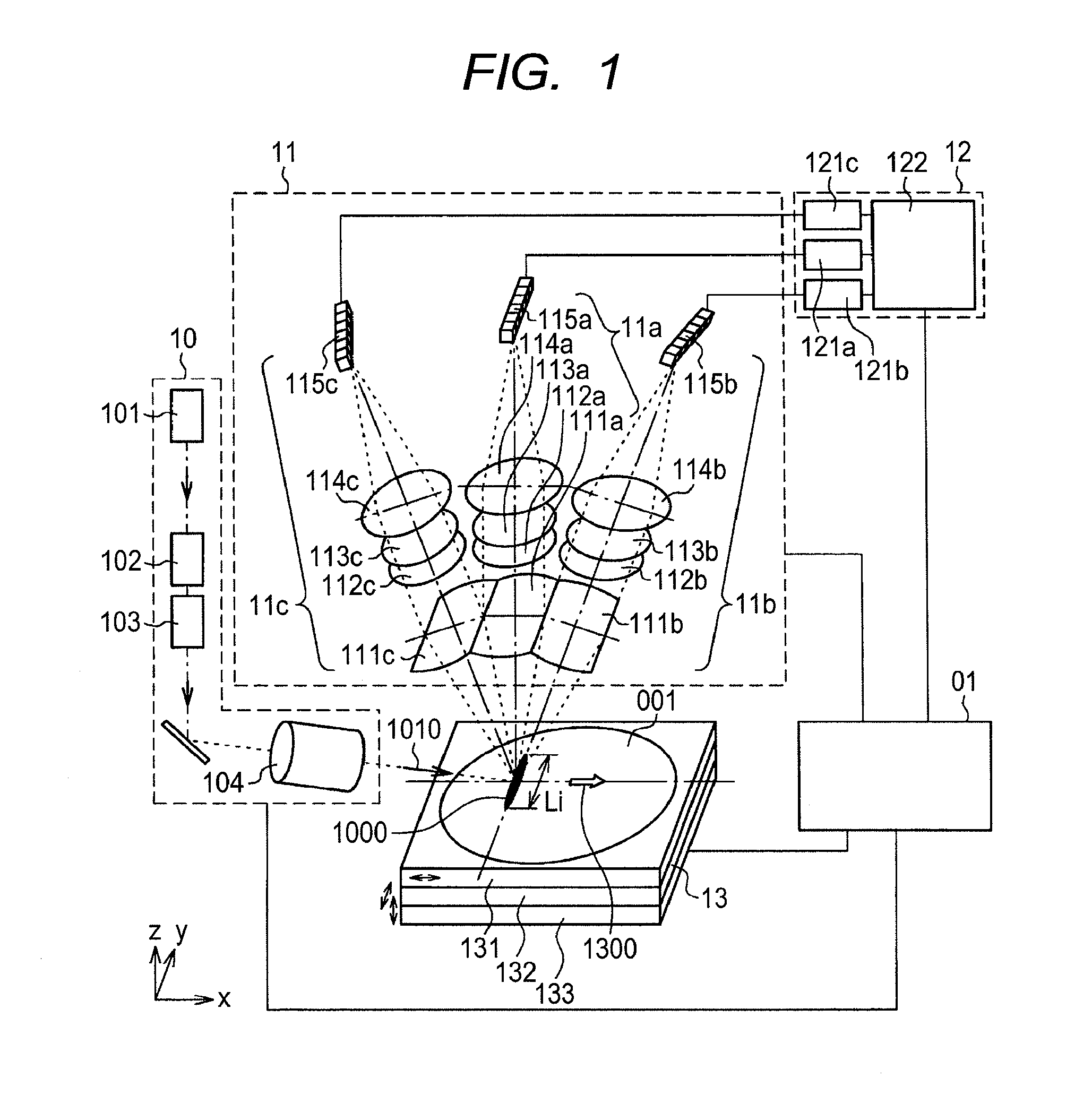
[0056]FIG. 1 shows an example of a defect inspection device configuration as a first embodiment. The defect inspection device according to the present embodiment includes an illumination optics unit 10, a detection optics unit 11, a data-processing unit 12, a stage unit 13, and a total control unit 01.

[0057]The illumination optics unit 10 includes a light source 101, a polarization state controller 102, a beam-forming unit 103, and a thin-line converging optics system 104. Illumination light that has emitted from the light source 101 in this configuration is passed through the polarization state controller 102 and the beam-forming unit 103, and then introduced into the thin-line converging optics system 104. The polarization state controller 102 is a member including such polarizers as a half-wave plate and a quarter-wave plate. The polarization state controller 102, further fitted with a driving element (not shown) that is adapted to rotate about an optical axis of the illumination...

second embodiment

[0107]Changes in ambient environment significantly affect the image quality of the scattered light. Although changes in temperature can be accommodated by merely providing a temperature control mechanism inside the device, it is difficult in terms of costs to provide, against changes in atmospheric pressure, a structure or mechanism that keeps an internal atmospheric pressure of the entire device constant.

[0108]FIGS. 9A and 9B are diagrams that explain impacts of atmospheric pressure changes upon the deterioration of image quality. FIG. 9A shows calculation results that indicate how changes in atmospheric pressure vary lens aberration. For example, even if a lens is assembled and adjusted under an environment of 1,000 hPa and aberration is controlled below 0.1λ, a decrease of the atmospheric pressure to 850 hPa degrades aberration to 0.2λ.

[0109]The degradation in aberration is a component that cannot be sufficiently corrected by adjustment of the imaging position, as in the prior-ar...

third embodiment

[0134]A third embodiment relates to a direction of illumination. As described earlier herein, the present embodiment presupposes that the longitudinal direction of the thin linear illumination region 1000 is set to be the y-axis direction, but this is not intended to limit the direction of the illumination.

[0135]Constituent elements of the present embodiment, such as the illumination optics unit 10 and the detection optics system 11, are substantially the same as in the defect inspection device of the first embodiment described using FIG. 1, and the present (third) embodiment differs from the first embodiment in terms of a location of the illumination optics unit 10 relative to the detection optics system 11.

[0136]As shown in FIG. 11, a plane 1010, formed by a line 1111 normal to a surface of a wafer 001 and an optical axis of the illumination light, may have an arbitrary azimuth angle “φi” with respect to the y-axis. Thus, as described earlier herein, different scattered-light comp...


PUM


Abstract

A defect inspection method and device for irradiating a linear region on a surface-patterned sample mounted on a table, with illumination light from an inclined direction to the sample, next detecting in each of a plurality of directions an image of the light scattered from the sample irradiated with the illumination light, then processing signals obtained by the detection of the images of the scattered light, and thereby detecting a defect present on the sample; wherein the step of detecting the scattered light image in the plural directions is performed through oval shaped lenses in which elevation angles of the optical axes thereof are different from each other, within one plane perpendicular to a plane formed by the normal to the surface of the table on which to mount the sample and the longitudinal direction of the linear region irradiated with the irradiation light.

Description

BACKGROUND[0001]The present invention relates generally to inspection techniques that use optically acquired image signal information to detect defects present on a surface-patterned object to be inspected. More particularly, the invention is directed to an inspection technique for detecting microscopic defects present on a patterned substrate such as a semiconductor wafer.[0002]In defect inspection of a substrate having patterns formed on a surface (i.e., a patterned substrate), defect detection sensitivity depends greatly upon how accurately a defect-diffracted / scattered detection beam of light, or a defect signal, can be detected in distinction from pattern-diffracted / scattered and underlayer-diffracted / scattered detection beams of light, or background light noise. During the inspection of a semiconductor wafer, in particular, the detection of even more microscopic defects is being demanded in response to the progress of further microstructured patterning, and how accurately a ve...

Claims


Application Information

Patent Timeline
IPC IPC(8): G01N21/95G01N21/956
CPCG01N21/9501G01N2201/127G01N2201/126G01N21/956H01L22/12H01L2924/0002H01L2924/00
Inventor MATSUMOTO, SHUNICHITANIGUCHI, ATSUSHIHONDA, TOSHIFUMISHIBATA, YUKIHIROURANO, YUTA
Owner HITACHI HIGH-TECH CORP
Why Eureka
Try Eureka