Method for measuring clearance in proximity nanometer lithography

A technology of nano-lithography and measurement methods, which is applied in measurement devices, optical devices, instruments, etc., to achieve the effect of improving precision and improving anti-interference ability

Inactive Publication Date: 2010-11-03
INST OF OPTICS & ELECTRONICS - CHINESE ACAD OF SCI
View PDF3 Cites 14 Cited by
  • Summary
  • Abstract
  • Description
  • Claims
  • Application Information

AI Technical Summary

Problems solved by technology

[0004] The technical problem to be solved in the present invention is: to overcome the weakness in principle of the existing gap measurement method, further improve the gap measurement accuracy, and at the same time overcome the influence of photoresist and other silicon wafer processes on gap measurement, and provide a proximity nanometer In-etch gap measurement method to accommodate increasing resolution of nanolithography

Method used


Image

  • Method for measuring clearance in proximity nanometer lithography
  • Method for measuring clearance in proximity nanometer lithography
  • Method for measuring clearance in proximity nanometer lithography

Examples


Embodiment Construction

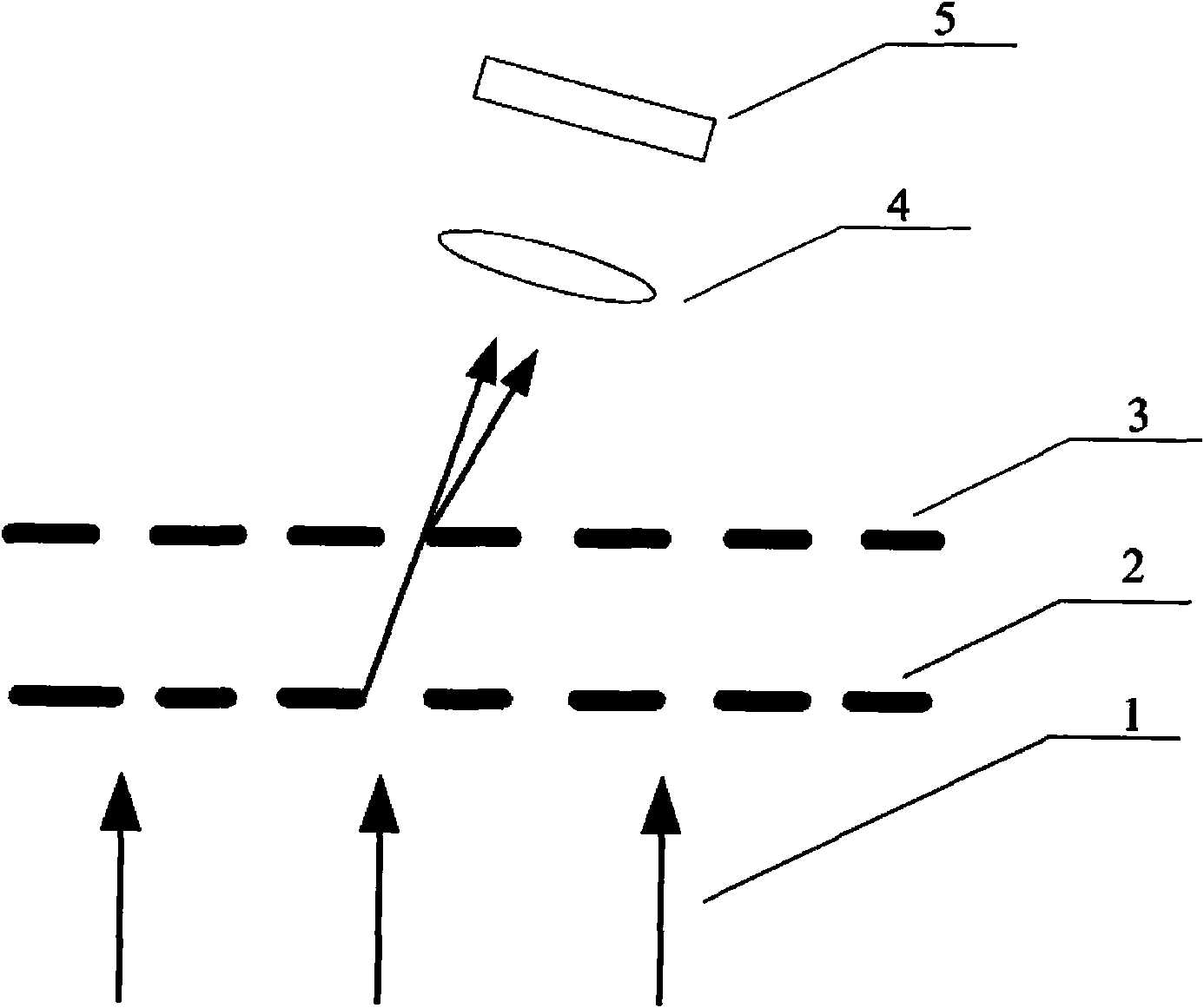
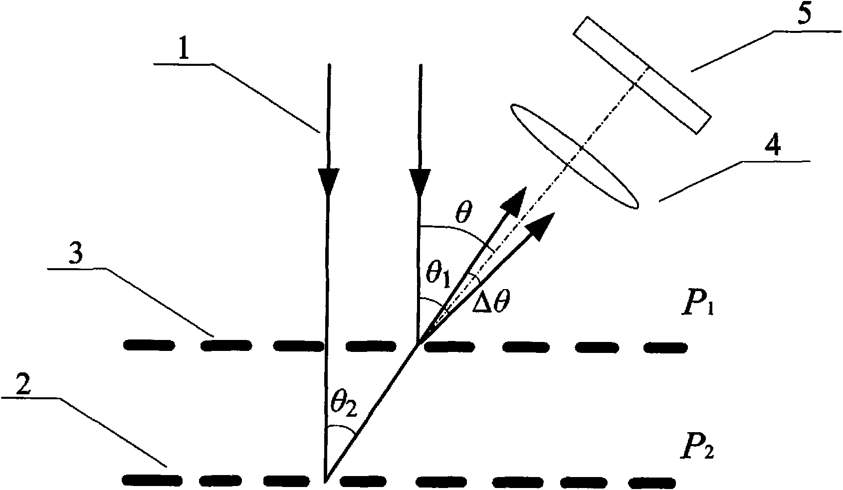
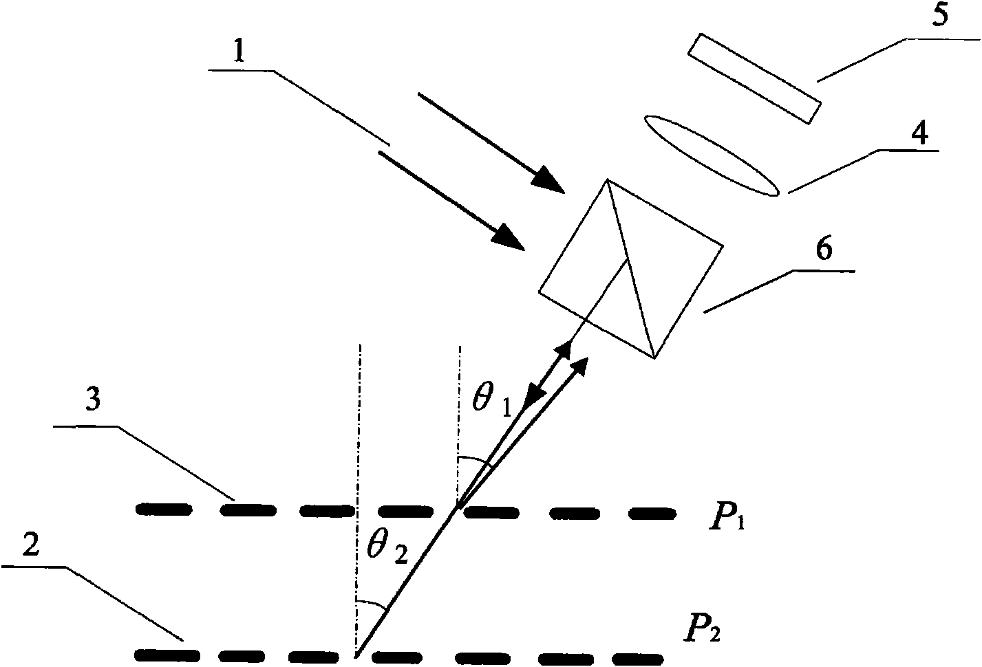
[0036] Such as figure 1 and figure 2 As shown, the gap measurement method applied between the mask and the transparent substrate of the present invention is:

[0037] First, grating 2 and grating 3 are respectively used as marking gratings for gap measurement on the silicon mask. Diffraction occurs on the grating 3. The diffracted lights of the same order from the two gratings (the +1 order is taken as an example in this embodiment, and other orders are similar) meet and interfere on the surface of the mask grating 3, producing interference fringes whose phase can change with the gap. For two beams of +n diffracted light, the interference field strength can be expressed as (maybe let the grating be distributed along the x direction)

[0038]

[0039] Among them, I 1 =a n 2 , I 2 =b n 2 is the intensity of two beams of +n diffracted light, is the initial phase, P=P 1 P 2 / [n(P 2 -P 1 )] is the distribution period of two +n diffracted light interference fringe...


PUM


Abstract

The invention discloses a method for measuring clearance in proximity nanometer lithography and mainly aims at the controlling of the clearance of a masking silicon wafer in nanometer manufacturing technology, such as nano-imprint, wave zone plate array imaging and the like. The basic process of the method can be simply explained in the picture 1 that: incident plane waves pass through a silicon wafer gratings and a mask grating and diffract for multiple times, wherein the two periods of the gratings are approximate and the two gratings are overlapped with a certain gap; two beams of lateral diffracted light from the two gratings interfere with each other and are superposed, and form Moire interference fringes of which the period is amplified relative to the conventional gratings on the surfaces of the silicon wafer grating; and the fringes are imaged on a CCD image detector through an objective lens with certain multiplying power. The change of the gap between the two gratings causes the change of optical path difference of the two beams and then causes the change of the movement or phases of the interference fringes so that the aim of measuring the gap is fulfilled; the more approximate the period is, the higher the sensitivity of the measurement is; and, at the same time, because the periods of the two gratings are approximate, the included angle between the lateral diffracted light is very small, the frequency of the interference fringes is very low (namely, the period is long), and the requirement on the numerical aperture of the objective lens is low. With the development of microfabrication technology, the machining accuracy of the grafting is higher and the method has great significance for gap measurement in proximity nanometer lithography and the related field.

Description

technical field [0001] The invention relates to a gap measurement method used in proximity nanolithography, and belongs to the related fields of micro-nano processing and high-precision measurement. Background technique [0002] Optical lithography has always been the basis of large-scale integrated circuit industrial manufacturing technology. With the development of highly integrated circuits and related devices, IC feature sizes are getting smaller and smaller, and high-resolution lithography technology has been greatly developed. In addition, the rapid development of nanotechnology and the continuous reduction of the feature size of nanodevices have also promoted the development of nanolithography technology, such as nanoimprinting and zone plate array imaging lithography. Correspondingly, with the improvement of resolution and the adoption of large-size silicon wafers, the gap control and measurement of mask silicon wafers will become a severe challenge for proximity lit...

Claims


Application Information

Patent Timeline
Patent Type & Authority Applications(China)
IPC IPC(8): G01B11/14G01B9/021
Inventor 周绍林胡松唐小萍赵立新杨勇徐锋陈旺富陈明勇
Owner INST OF OPTICS & ELECTRONICS - CHINESE ACAD OF SCI
Why Eureka
Try Eureka