Photodetector

a photodetector and detector technology, applied in the field of photodetectors, can solve the problems of inability to improve the s/n ratio, the bulky size of the photomultiplier tube, and the inability to make the array, so as to reduce the length and width of the channel, the effect of high speed and reduced channel width

Inactive Publication Date: 2005-07-14
NAT INST OF ADVANCED IND SCI & TECH
View PDF3 Cites 17 Cited by
  • Summary
  • Abstract
  • Description
  • Claims
  • Application Information

AI Technical Summary

Benefits of technology

[0024] Because the photosensitive region and charge detection FET are separated in the photodetector embodied in this invention, optimal design can be pursued at the respective regions. High speed and high sensitive detection of photogenerated carriers is achieved by the reduction of channel length and channel width.
[0025] This photodetector has an advantage of avoiding exogenous noise because the photosensitive region and charge detection FET are interconnected each other inside of the device structure. Cryogenic operation is favorable for high sensitive photon detection by increasing the photogenerated electron-hole recombination lifetime.

Problems solved by technology

However, photo-multiplier tubes are bulky and cannot be made into arrays.
For high-sensitivity physical measurement of such wavelengths, devices are frequently cooled down to prevent degradation of sensitivity induced by a thermal noise, which causes additional complexity in the apparatus and increased production costs.
However, this cannot improve the S / N ratio in short exposure times.
However, 1 G bit / s has been the maximum bit rate, limited by the recovery time from the avalanche multiplication of the photogenerated electrons.
Such complexity is inevitable in the system with the PIN diode because the quantum efficiency of the PIN diode is physically limited to 1 (approximately 1 A / W): one photon generates only one pair of electron and hole.
That is, the response speed deteriorates as the sensitivity increases.
Its sensitivity goes up close to infinity, although it is not easy to control its performance.
Improving both sensitivity and response speed is a difficult task in general.
However, micro-fabrication techniques can effectively reduce the device's capacitance and resistance and improve its performance.
In the device disclosed in non-patent reference document 1, detection of induced charge is inefficient because the conducting channel of the FET is two-dimensional.
In non-patent reference document 2, although it is advantageous that charge accumulation and charge read out regions are constructed three-dimensionally, the use of oblique side walls on the higher-order substrate restricts the selection of constituent materials, limits circuit design, and causes high power dissipation in the read-out FET due to poor electron mobility along the channel.
Large parasitic capacitance becomes an obstacle for the high speed operation of photodetectors as well.
The regrowth process induces interface defects especially in the aluminum containing materials, such as AlGaAs, which cause instability in device operation.

Method used


Image

  • Photodetector
  • Photodetector
  • Photodetector

Examples


Embodiment Construction

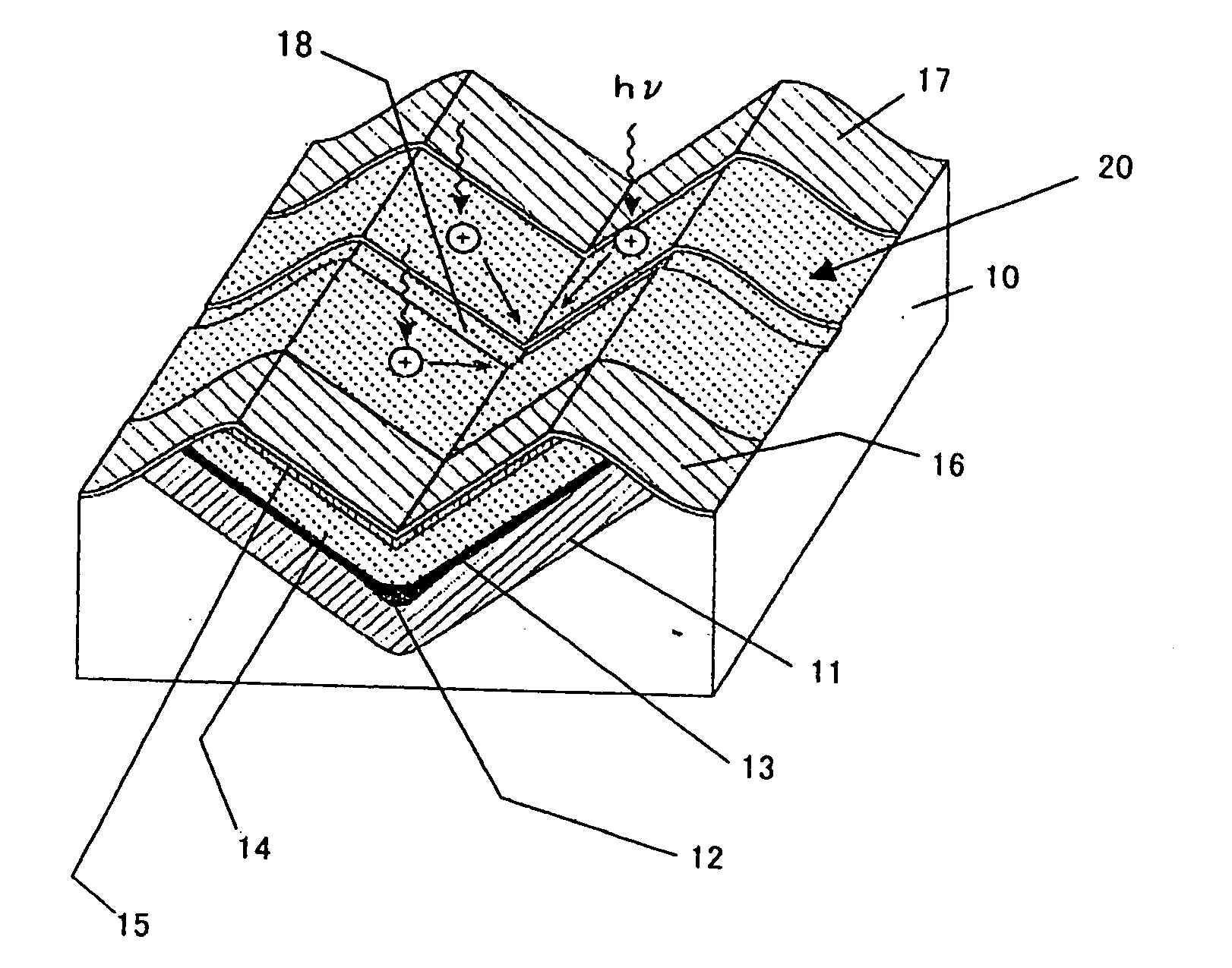
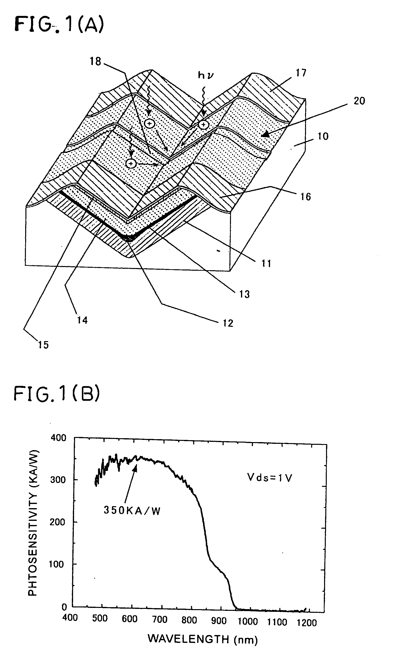
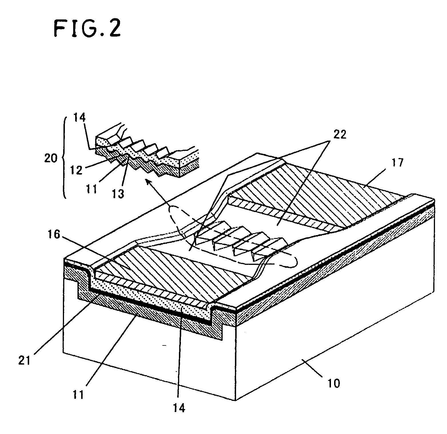
[0035]FIG. 1(A) shows the schematic structure of one embodiment of a photodetector constituted according to the present invention. In this case, the V-grooved substrate 10 is assumed to have been made by forming a V-shaped groove in a GaAs or InP substrate. A known method of forming such a V-shaped groove may be used; for example, by forming a 0.2-2 μm resist pattern in the [0-10] orientation upon a (100) GaAs substrate and then using an aqueous ammonia-hydrogen peroxide solution (ammonia:hydrogen peroxide:water=1:3:50) or the like to perform wet etching with high dependence on the crystal orientation.

[0036] This V-grooved substrate 10 is sequentially subjected to a series of operations. For example, a single run of MOCVD deposition can be used to form: an undoped AlGaAs lower clad layer 11, a GaAs or InGaAs quantum wire 12, an intervening undoped AlGaAs spacer layer (not shown), a silicon-doped AlGaAs upper clad layer 14, and a silicon-doped GaAs cap layer 15. Here, the deposition...


PUM


Abstract

Quantum wire is formed on the bottom of a V-shaped groove in a V-grooved substrate as a channel between source and drain electrodes or as at least part of the channel. A photocarrier accumulation region is provided within the quantum wire or at a position connected to or adjacent to the quantum wire for accumulating charges generated when light shines onto a photosensitive region that comprises at least a clad layer that covers the quantum wire. A recess is provided in the upper clad layer to localize the photocarrier accumulation region. As a result, it is possible to provide a photodetector that exhibits high sensitivity, high speed and low power consumption in an expanded wavelength region. It is also possible to provide a photodetector capable of constructing core portions thereof by one-time selective growth.

Description

BACKGROUND OF THE INVENTION [0001] 1. Field of the Invention [0002] The present invention relates to a photodetector used to detect very weak optical signals. More specifically, the invention relates to an ultra-high sensitivity, high-performance, high-speed and low-power consumption photodetector that operates in the ultraviolet, visible and infrared regions, which are important in the fields of scientific instruments, telecommunications and general consumer products. [0003] 2. Description of the Prior Art [0004] The various designs for photodetectors may be categorized into photodiodes in which photocarriers at a semiconductor photosurface are simply transformed into photo-current, avalanche photodiodes in which photocarriers are accelerated and multiplied, photo-FETs in which photocarriers are accumulated underneath the gate regions and amplified, and photo-multiplier tubes in which photoelectrons are multiplied. The silicon photodiode is most suitable and less expensive in the s...

Claims


Application Information

Patent Timeline
Patent Type & Authority Applications(United States)
IPC IPC(8): H01L31/10H01L31/00
CPCB82Y10/00H01L31/035236B82Y20/00
Inventor OGURA, MUTSUONAGAMUNE, YASUSHISUGAYA, TAKEYOSHI
Owner NAT INST OF ADVANCED IND SCI & TECH
Why Eureka
Try Eureka