Real-time adaptive SRAM array for high SEU immunity

a real-time adaptive, seu-adjustable technology, applied in static storage, digital storage, instruments, etc., can solve the problems of array access times, overkill design approach taken by the industry to provide acceptable seu-adjustable immunity, etc., and achieve the effect of maximizing cell performan

Inactive Publication Date: 2007-10-16
GOOGLE LLC
View PDF4 Cites 53 Cited by
  • Summary
  • Abstract
  • Description
  • Claims
  • Application Information

AI Technical Summary

Benefits of technology

[0016]Once the radiation characteristics of the environment are determined by the SRAM sensing sub-array, one or more of the above mentioned electrical parameters may be adjusted in the primary SRAM arrays. For the primary SRAM arrays, combinations of the beta ratio, N-well bias, and the power supply of the cell can be dynamically adjusted to assure immunity to upsets of the internal latched state of the SRAM cells caused by an ionizing particles, while maximizing the cell performance.

Problems solved by technology

In single event upsets (SEU) due to ionizing events caused by comic rays, particles from terrestrial sources, and materials in proximity to the chip present a reliability challenge to semiconductor memories (e.g. SRAM, DRAM) and logic circuits.
The approach taken by the industry to provide acceptable immunity to SEU has been overkill in design.
The price for this conservative design is compromised performance, specifically, array access times. Once designed, the SEU exposure of these SRAM is frozen.
Due to the existing off-set, the cell is susceptible to be upset by heavy ion events.
There are at least three disadvantages of this design: (1) The cell is inherently unbalanced; even when Vo=Vdd, the cell is still not fully balanced since two inverters are connected to two different power supplies.
(2) This SRAM array can only be used as a particle monitor and cannot be used in normal operation with high reliability.
(3) Since the cell has a built-in off-set, it is vulnerable to other types of errors such as read and / or write disturbances.
Therefore, it would be difficult to distinguish whether the bit error is caused by radiation induced soft-error or other types of error mechanism.
While using two identical arrays to catch and correct soft error is advantageous, it provides no means for speeding up error rate detection.
However, this reference provides no means for improving the reliability of memory arrays by determining the actual SEU exposure to a given radiation environment; rather, the focus of this device is to boost the immunity to radiation induced upset on CMOS logic circuits.

Method used


Image

  • Real-time adaptive SRAM array for high SEU immunity
  • Real-time adaptive SRAM array for high SEU immunity
  • Real-time adaptive SRAM array for high SEU immunity

Examples


Embodiment Construction

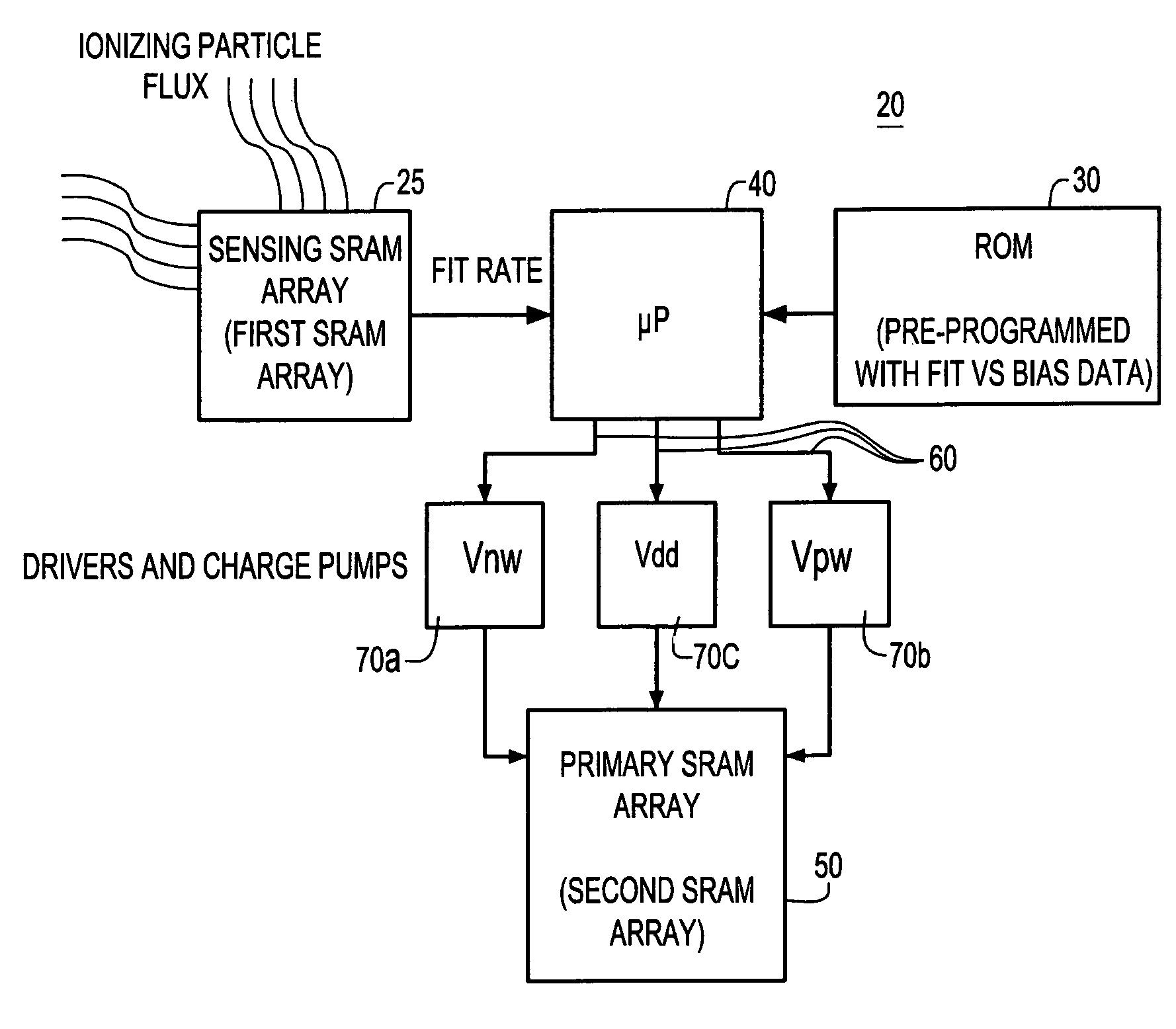
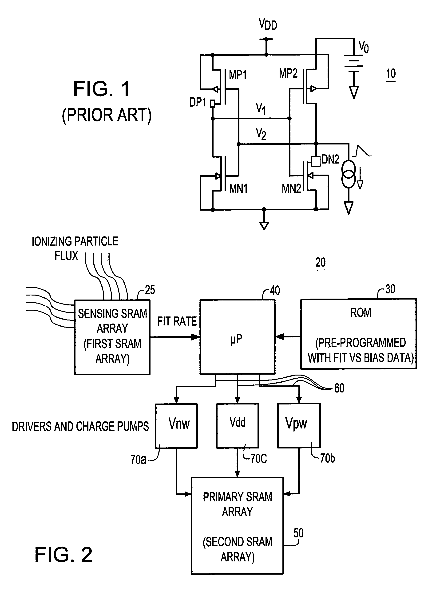
[0043]The present invention provides a system and method for automatically adjusting one or more electrical parameters in memory, e.g., SRAM arrays, and more particularly, a novel system and method for setting the SEU sensitivity of a primary SRAM memory array to a predetermined fail rate in an ionizing particle environment. The predetermined fail rate is maintained on a real-time basis in order to provide immunity to SEU consistent with optimum performance.

[0044]A block diagram of the inventive system 20 is illustrated in FIG. 2. As shown in FIG. 2, a first SRAM memory array 25 (sensing sub-array) is provided for the purpose of collecting accelerated SEU data from its interaction with the particles in the ionizing particle flux environment. The above-mentioned SEU data is then applied to a reliability algorithm for determining the electrical operating conditions required to obtain a predetermined SEU fail rate for a second (primary) SRAM array 50. The reliability algorithm determin...


PUM


Abstract

A system and method for automatically adjusting one or more electrical parameters in a memory device, e.g., SRAM arrays. The system and method implements an SRAM sensing sub-array for accelerated collection of fail rate data for use in determining the operating point for optimum tradeoff between single event upset immunity and performance of a primary SRAM array. The accelerated fail rate data is input to an algorithm implemented for setting the SEU sensitivity of a primary SRAM memory array to a predetermined fail rate in an ionizing particle environment. The predetermined fail rate is maintained on a real-time basis in order to provide immunity to SEU consistent with optimum performance.

Description

BACKGROUND OF THE INVENTION[0001]1. Field of the Invention[0002]The present invention relates generally to semiconductor memory structures, e.g., SRAM, and particularly, an SRAM cell structure, array architecture and method of operation which provides a real-time adaptive tradeoff between immunity to single event upset (SEU) due to ionizing particles (including proton, neutron, pion, alpha particle, or heavy ions) and performance.[0003]2. Description of the Prior Art[0004]In single event upsets (SEU) due to ionizing events caused by comic rays, particles from terrestrial sources, and materials in proximity to the chip present a reliability challenge to semiconductor memories (e.g. SRAM, DRAM) and logic circuits. High performance SRAM sensitivity to cosmic rays—measured on the basis of fails per bit—has dropped by about 10× over the last 15 years, while the bits / chip has increased 1000×; hence the net fail rate per chip has increased about 100 times. Modern CMOS chips are increasingl...

Claims


Application Information

Patent Timeline
Patent Type & Authority Patents(United States)
IPC IPC(8): G11C7/00
CPCG11C11/4125
Inventor HSU, LOUIS L.MANDELMAN, JACK A.WONG, ROBERT C.YANG, CHIH-CHAO
Owner GOOGLE LLC
Why Eureka
Try Eureka